SNVSAZ4A February 2021 – March 2021 TPS541620
PRODUCTION DATA
- 1 Features
- 2 Applications
- 3 Description
- 4 Revision History
- 5 Pin Configuration and Functions
- 6 Specifications
-
7 Detailed Description
- 7.1 Overview
- 7.2 Functional Block Diagram
- 7.3
Feature Description
- 7.3.1 Fixed-Frequency, Internally Compensated Advanced-Current-Mode Control
- 7.3.2 Enable and UVLO
- 7.3.3 Internal LDO
- 7.3.4 Pre-biased Output Start-up
- 7.3.5 Current Sharing
- 7.3.6 Frequency Selection and Minimum On-Time and Off-Time
- 7.3.7 Ramp Compensation Selection
- 7.3.8 Soft Start
- 7.3.9 Remote Sense Function
- 7.3.10 Adjustable Output Voltage
- 7.3.11 Power Good
- 7.3.12 Overcurrent Protection
- 7.3.13 Overvoltage and Undervoltage Protection
- 7.3.14 Overtemperature Protection
- 7.3.15 Frequency Synchronization
- 7.4 Device Functional Modes
-
8 Application and Implementation
- 8.1 Application Information
- 8.2
Typical Application - Dual Independent Outputs
- 8.2.1 Design Requirements
- 8.2.2
Detailed Design Procedure
- 8.2.2.1 Switching Frequency
- 8.2.2.2 Output Inductor Selection
- 8.2.2.3 Output Capacitor
- 8.2.2.4 Input Capacitor
- 8.2.2.5 Output Voltage Resistors Selection
- 8.2.2.6 Adjustable Undervoltage Lockout
- 8.2.2.7 Bootstrap Capacitor Selection
- 8.2.2.8 BP5 Capacitor Selection
- 8.2.2.9 PGOOD Pullup Resistor
- 8.2.2.10 Current Limit
- 8.2.2.11 Soft-Start Time Selection
- 8.2.2.12 MODE1 and MODE2 Pins
- 8.2.3 Application Curves
- 8.2.4
Typical Application - 2-Phase Operation
- 8.2.4.1 Design Requirements
- 8.2.4.2
Detailed Design Procedure
- 8.2.4.2.1 Switching Frequency
- 8.2.4.2.2 Output Inductor Selection
- 8.2.4.2.3 Output Capacitor
- 8.2.4.2.4 Input Capacitor
- 8.2.4.2.5 Output Voltage Resistors Selection
- 8.2.4.2.6 Adjustable Undervoltage Lockout
- 8.2.4.2.7 Bootstrap Capacitor Selection
- 8.2.4.2.8 BP5 Capacitor Selection
- 8.2.4.2.9 PGOOD Pullup Resistor
- 8.2.4.2.10 Current Limit
- 8.2.4.2.11 Soft-Start Time Selection
- 8.2.4.2.12 MODE1 Pin
- 8.2.4.3 Application Curves
- 9 Power Supply Recommendations
- 10Layout
- 11Device and Documentation Support
- 12Mechanical, Packaging, and Orderable Information
Package Options
Mechanical Data (Package|Pins)
- RPB|25
Thermal pad, mechanical data (Package|Pins)
Orderable Information
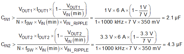
8.2.2.4 Input Capacitor
It is required to have input decoupling ceramic capacitors type X5R, X7R, or similar from both the PVIN1 and PVIN2 pins to PGND to bypass the power-stage and be placed as close as possible. A total of at least 10 µF of capacitance is required. Some applications can require a bulk capacitance. At least 1 µF of bypass capacitance is recommended near both VIN pins to minimize the input voltage ripple. A 0.1-µF to 1-µF capacitor must be placed by both PVIN1 and PVIN2 pins 8 and 12 to provide high frequency bypass to reduce the high frequency overshoot and undershoot on the following pins:
- PVIN1
- SW1
- PVIN2
- SW2
For this example design, a ceramic capacitor with at least a 16-V voltage rating is required to support the maximum input voltage. Two 10-µF, 0805, X7S, 25-V and two 0.1-μF, 0402, X7R 50-V capacitors in parallel have been selected to be placed on both sides of the IC near both PVIN pins to PGND pins. Based on the capacitor manufacturer's website, the total ceramic input capacitance derates to 5.4 µF at the nominal input voltage of 12 V. A 100-µF bulk capacitance is also used to bypass long leads when connected a lab bench top power supply.
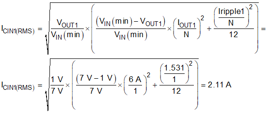
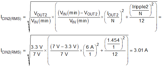
The input capacitance value determines the input ripple voltage of the regulator. The input voltage ripple can be calculated using Equation 37. The maximum input ripple occurs when operating nearest to 50% duty cycle. Using the nominal design example values of IOUT1 = 6 A, fSW = 1000 kHz, VOUT1 the input voltage ripple with the 12-V nominal input is 350 mV, and the RMS input ripple current with the 7-V minimum input is 2.106 A. Similarly, for VOUT2, the input RMS current is 3.01 A.
For applications requiring bulk capacitance on the input, such as ones with low input voltage and high current, the selection process in the How To Select Input Capacitors For A Buck Converter technical brief is recommended.