SNVSAZ4A February 2021 – March 2021 TPS541620
PRODUCTION DATA
- 1 Features
- 2 Applications
- 3 Description
- 4 Revision History
- 5 Pin Configuration and Functions
- 6 Specifications
-
7 Detailed Description
- 7.1 Overview
- 7.2 Functional Block Diagram
- 7.3
Feature Description
- 7.3.1 Fixed-Frequency, Internally Compensated Advanced-Current-Mode Control
- 7.3.2 Enable and UVLO
- 7.3.3 Internal LDO
- 7.3.4 Pre-biased Output Start-up
- 7.3.5 Current Sharing
- 7.3.6 Frequency Selection and Minimum On-Time and Off-Time
- 7.3.7 Ramp Compensation Selection
- 7.3.8 Soft Start
- 7.3.9 Remote Sense Function
- 7.3.10 Adjustable Output Voltage
- 7.3.11 Power Good
- 7.3.12 Overcurrent Protection
- 7.3.13 Overvoltage and Undervoltage Protection
- 7.3.14 Overtemperature Protection
- 7.3.15 Frequency Synchronization
- 7.4 Device Functional Modes
-
8 Application and Implementation
- 8.1 Application Information
- 8.2
Typical Application - Dual Independent Outputs
- 8.2.1 Design Requirements
- 8.2.2
Detailed Design Procedure
- 8.2.2.1 Switching Frequency
- 8.2.2.2 Output Inductor Selection
- 8.2.2.3 Output Capacitor
- 8.2.2.4 Input Capacitor
- 8.2.2.5 Output Voltage Resistors Selection
- 8.2.2.6 Adjustable Undervoltage Lockout
- 8.2.2.7 Bootstrap Capacitor Selection
- 8.2.2.8 BP5 Capacitor Selection
- 8.2.2.9 PGOOD Pullup Resistor
- 8.2.2.10 Current Limit
- 8.2.2.11 Soft-Start Time Selection
- 8.2.2.12 MODE1 and MODE2 Pins
- 8.2.3 Application Curves
- 8.2.4
Typical Application - 2-Phase Operation
- 8.2.4.1 Design Requirements
- 8.2.4.2
Detailed Design Procedure
- 8.2.4.2.1 Switching Frequency
- 8.2.4.2.2 Output Inductor Selection
- 8.2.4.2.3 Output Capacitor
- 8.2.4.2.4 Input Capacitor
- 8.2.4.2.5 Output Voltage Resistors Selection
- 8.2.4.2.6 Adjustable Undervoltage Lockout
- 8.2.4.2.7 Bootstrap Capacitor Selection
- 8.2.4.2.8 BP5 Capacitor Selection
- 8.2.4.2.9 PGOOD Pullup Resistor
- 8.2.4.2.10 Current Limit
- 8.2.4.2.11 Soft-Start Time Selection
- 8.2.4.2.12 MODE1 Pin
- 8.2.4.3 Application Curves
- 9 Power Supply Recommendations
- 10Layout
- 11Device and Documentation Support
- 12Mechanical, Packaging, and Orderable Information
Package Options
Mechanical Data (Package|Pins)
- RPB|25
Thermal pad, mechanical data (Package|Pins)
Orderable Information
8.2.2.1 Switching Frequency
The first step is to decide on a switching frequency. The TPS541620 can operate at four different frequencies from 500 kHz to 2.0 MHz. fSW is set by the resistor value from the MODE2 pin to ground. Typically, the highest switching frequency possible is desired because it produces the smallest solution size or lower switching frequency for a more efficient converter. The minimum controllable on-time and maximum off-time affect the input voltage range and switching frequency.
The maximum switching frequency for a given application can be limited by the minimum on-time of the regulator and the maximum fSW can be estimated with Equation 22. Using the minimum 50-ns on-time, 15-V maximum input voltage, and the lower voltage of the dual-output 1 V for this application, the maximum switching frequency is 1333 kHz. The minimum regulating input voltage is limited by the maximum off-time, switching frequency, and output voltage. Using the maximum off-time of 150 ns, 7-V minimum input voltage, and the higher voltage of the dual-output 3.3 V for this application with Equation 4, the maximum switching frequency from 3.3 V and maximum off-time is 3524 kHz.
The selected switching frequency must also consider the tolerance of the switching frequency. A switching frequency of 1000 kHz is selected for a good balance of solution size and efficiency. To set the frequency to 1000 kHz, the selected MODE2 resistor is 17.4 kΩ per Table 7-1. To set for dual-output configuration, select a MODE1 resistor is 15.4 kΩ per Table 7-3.
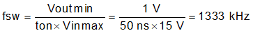
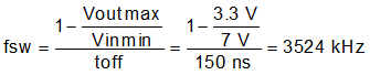
Figure 8-2 shows the maximum recommended input voltage versus output voltage for each frequency. Figure 8-2 uses the maximum minimum on-time of 50 ns and includes 10% tolerance on the switching frequency.
 Figure 8-2 Maximum Input Voltage Versus Output
Voltage
Figure 8-2 Maximum Input Voltage Versus Output
Voltage