SLVSDG7A April 2016 – April 2021 TPS54202H
PRODUCTION DATA
- 1 Features
- 2 Applications
- 3 Description
- 4 Revision History
- 5 Pin Configuration and Functions
- 6 Specifications
-
7 Detailed Description
- 7.1 Overview
- 7.2 Functional Block Diagram
- 7.3
Feature Description
- 7.3.1 Fixed-Frequency PWM Control
- 7.3.2 Pulse Skip Mode
- 7.3.3 Error Amplifier
- 7.3.4 Slope Compensation and Output Current
- 7.3.5 Device Enable
- 7.3.6 Adjusting Under Voltage Lockout
- 7.3.7 Safe Startup into Pre-Biased Outputs
- 7.3.8 Voltage Reference
- 7.3.9 Adjusting Output Voltage
- 7.3.10 Internal Soft-Start
- 7.3.11 Bootstrap Voltage (BOOT)
- 7.3.12 Overcurrent Protection
- 7.3.13 Output Overvoltage Protection (OVP)
- 7.3.14 Thermal Shutdown
- 7.4 Device Functional Modes
- 8 Application and Implementation
- 9 Power Supply Recommendations
- 10Layout
- 11Device and Documentation Support
- 12Mechanical, Packaging, and Orderable Information
Package Options
Mechanical Data (Package|Pins)
- DDC|6
Thermal pad, mechanical data (Package|Pins)
Orderable Information
8.2.3.3 Output Voltage Set Point
The output voltage of the TPS54202H device is externally adjustable using a resistor divider network. In the application circuit of , this divider network is comprised of R2 and R3. Use Equation 6 and Equation 7 to calculate the relationship of the output voltage to the resistor divider.
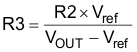
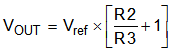
Select a value of R2 to be approximately 100 kΩ. Slightly increasing or decreasing R3 can result in closer output voltage matching when using standard value resistors. In this design, R2 = 100 kΩ and R3 = 13.3 kΩ which results in a 5-V output voltage. The 49.9-Ω resistor, R1, is provided as a convenient location to break the control loop for stability testing.