SLVSDG7A April 2016 – April 2021 TPS54202H
PRODUCTION DATA
- 1 Features
- 2 Applications
- 3 Description
- 4 Revision History
- 5 Pin Configuration and Functions
- 6 Specifications
-
7 Detailed Description
- 7.1 Overview
- 7.2 Functional Block Diagram
- 7.3
Feature Description
- 7.3.1 Fixed-Frequency PWM Control
- 7.3.2 Pulse Skip Mode
- 7.3.3 Error Amplifier
- 7.3.4 Slope Compensation and Output Current
- 7.3.5 Device Enable
- 7.3.6 Adjusting Under Voltage Lockout
- 7.3.7 Safe Startup into Pre-Biased Outputs
- 7.3.8 Voltage Reference
- 7.3.9 Adjusting Output Voltage
- 7.3.10 Internal Soft-Start
- 7.3.11 Bootstrap Voltage (BOOT)
- 7.3.12 Overcurrent Protection
- 7.3.13 Output Overvoltage Protection (OVP)
- 7.3.14 Thermal Shutdown
- 7.4 Device Functional Modes
- 8 Application and Implementation
- 9 Power Supply Recommendations
- 10Layout
- 11Device and Documentation Support
- 12Mechanical, Packaging, and Orderable Information
Package Options
Mechanical Data (Package|Pins)
- DDC|6
Thermal pad, mechanical data (Package|Pins)
Orderable Information
7.3.5 Device Enable
The EN pin provides electrical on and off control of the device. When the EN pin voltage exceeds the threshold voltage, the device begins operation. If the EN pin voltage is pulled below the threshold voltage, the regulator stops switching and enters the low-quiescent (IQ) state.
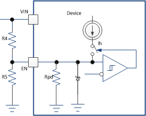
The EN pin has an internal pull down resistance Rpd (typical 1 MΩ) which allows the user to float the EN pin to disable the device, a Zener diode (typical break down voltage 6.9 V) is used to clamp the EN input voltage. To enable the device, connect a pull up resistor R4 (typical 510 KΩ) between EN and VIN, R4 is used to limit the quiet scent current of the device for light load efficiency improvement.
 Figure 7-1 Adjustable VIN Undervoltage Lockout