SLUS859C October 2008 – January 2015 TPS54233
PRODUCTION DATA.
- 1 Features
- 2 Applications
- 3 Description
- 4 Simplified Schematic
- 5 Revision History
- 6 Pin Configuration and Functions
- 7 Specifications
-
8 Detailed Description
- 8.1 Overview
- 8.2
Feature Description
- 8.2.1 Fixed Frequency PWM Control
- 8.2.2 Voltage Reference (Vref)
- 8.2.3 Bootstrap Voltage (BOOT)
- 8.2.4 Enable and Adjustable Input Under-Voltage Lockout (VIN UVLO)
- 8.2.5 Programmable Slow Start Using SS PIN
- 8.2.6 Error Amplifier
- 8.2.7 Slope Compensation
- 8.2.8 Current Mode Compensation Design
- 8.2.9 Overcurrent Protection and Frequency Shift
- 8.2.10 Overvoltage Transient Protection
- 8.2.11 Thermal Shutdown
- 8.3 Device Functional Modes
-
9 Application and Implementation
- 9.1 Application Information
- 9.2
Typical Application
- 9.2.1 Design Requirements
- 9.2.2 Detailed Design Procedure
- 9.2.3 Application Curves
- 10Power Supply Recommendations
- 11Layout
- 12Device and Documentation Support
- 13Mechanical, Packaging, and Orderable Information
Package Options
Mechanical Data (Package|Pins)
- D|8
Thermal pad, mechanical data (Package|Pins)
Orderable Information
7 Specifications
7.1 Absolute Maximum Ratings(1)
over operating free-air temperature range (unless otherwise noted)(1) Stresses beyond those listed under absolute maximum ratings may cause permanent damage to the device. These are stress ratings only, and functional operation of the device at these or any other conditions beyond those indicated under recommended operating conditions is not implied. Exposure to absolute-maximum-rated conditions for extended periods may affect device reliability.
7.2 ESD Ratings
| VALUE | UNIT | |||
|---|---|---|---|---|
| V(ESD) | Electrostatic discharge | Human-body model (HBM), per ANSI/ESDA/JEDEC JS-001(1) | ±2000 | V |
| Charged-device model (CDM), per JEDEC specification JESD22-C101(2) | ±500 | |||
(1) JEDEC document JEP155 states that 500-V HBM allows safe manufacturing with a standard ESD control process.
(2) JEDEC document JEP157 states that 250-V CDM allows safe manufacturing with a standard ESD control process.
7.3 Recommended Operating Conditions
over operating free-air temperature range (unless otherwise noted)| MIN | TYP | MAX | UNIT | |
|---|---|---|---|---|
| Operating Input Voltage on (VIN pin) | 3.5 | 28 | V | |
| Operating junction temperature, TJ | –40 | 150 | °C |
7.4 Thermal Information
| THERMAL METRIC(1) | D | UNIT | |
|---|---|---|---|
| 8 PINS | |||
| RθJA | Junction-to-ambient thermal resistance | 116.7 | °C/W |
| RθJC(top) | Junction-to-case (top) thermal resistance | 62.4 | |
| RθJB | Junction-to-board thermal resistance | 57.0 | |
| ψJT | Junction-to-top characterization parameter | 14.5 | |
| ψJB | Junction-to-board characterization parameter | 56.5 | |
| RθJC(bot) | Junction-to-case (bottom) thermal resistance | N/A | |
(1) For more information about traditional and new thermal metrics, see the IC Package Thermal Metrics application report, SPRA953.
7.5 Electrical Characteristics
TJ = –40°C to 150°C, VIN = 3.5V to 28V (unless otherwise noted)| PARAMETER | TEST CONDITIONS | MIN | TYP | MAX | UNIT |
|---|---|---|---|---|---|
| SUPPLY VOLTAGE (VIN PIN) | |||||
| Internal undervoltage lockout threshold | Rising and Falling | 3.5 | V | ||
| Shutdown supply current | EN = 0V, VIN = 12V, –40°C to 85°C | 1 | 4 | μA | |
| Operating – non switching supply current | VSENSE = 0.85 V | 75 | 110 | μA | |
| ENABLE AND UVLO (EN PIN) | |||||
| Enable threshold | Rising and Falling | 1.25 | 1.35 | V | |
| Input current | Enable threshold – 50 mV | -1 | μA | ||
| Input current | Enable threshold + 50 mV | -4 | μA | ||
| VOLTAGE REFERENCE | |||||
| Voltage reference | 0.772 | 0.8 | 0.828 | V | |
| HIGH-SIDE MOSFET | |||||
| On resistance | BOOT-PH = 3 V, VIN = 3.5 V | 115 | 200 | mΩ | |
| BOOT-PH = 6 V, VIN = 12 V | 80 | 150 | |||
| ERROR AMPLIFIER | |||||
| Error amplifier transconductance (gm) | –2 μA < I(COMP) < 2 μA, V(COMP) = 1 V | 92 | μmhos | ||
| Error amplifier DC gain(1) | VSENSE = 0.8 V | 800 | V/V | ||
| Error amplifier unity gain bandwidth(1) | 5 pF capacitance from COMP to GND pins | 2.7 | MHz | ||
| Error amplifier source/sink current | V(COMP) = 1 V, 100 mV overdrive | ±7 | μA | ||
| Switch current to COMP transconductance | VIN = 12 V | 9 | A/V | ||
| PULSE SKIPPING Eco-mode™ | |||||
| Pulse skipping Eco-mode™ switch current threshold | 100 | mA | |||
| CURRENT LIMIT | |||||
| Current limit threshold | VIN = 12 V | 2.3 | 3.5 | A | |
| THERMAL SHUTDOWN | |||||
| Thermal Shutdown | 165 | °C | |||
| SLOW START (SS PIN) | |||||
| Charge current | V(SS) = 0.4 V | 2 | μA | ||
| SS to VSENSE matching | V(SS) = 0.4 V | 10 | mV | ||
(1) Specified by design
7.6 Switching Characteristics
TJ = –40°C to 150°C, VIN = 3.5 to 28 V (unless otherwise noted)| PARAMETER | TEST CONDITIONS | MIN | TYP | MAX | UNIT | |
|---|---|---|---|---|---|---|
| SWITCHING FREQUENCY | ||||||
| Device switching frequency | VIN = 12 V | 210 | 300 | 390 | kHz | |
| Minimum controllable on time | VIN = 12 V, 25°C | 105 | 130 | ns | ||
| Maximum controllable duty ratio(1) | BOOT-PH = 6 V | 90% | 93% | |||
(1) Specified by design.
7.7 Typical Characteristics
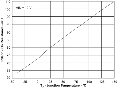 Figure 1. On Resistance vs Junction Temperature
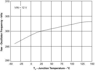 Figure 3. Switching Frequency vs Junction Temperature
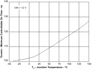 Figure 5. Minimum Controllable On Time vs
 Junction Temperature
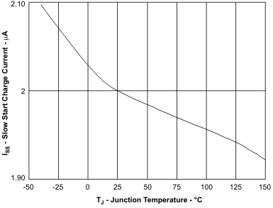 Figure 7. SS Charge Current vs Junction Temperature
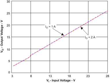 Figure 9. Typical Maximum Output Voltage vs
 Input Voltage
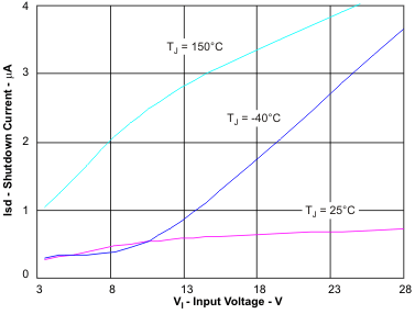 Figure 2. Shutdown Quiescent Current vs Input Voltage
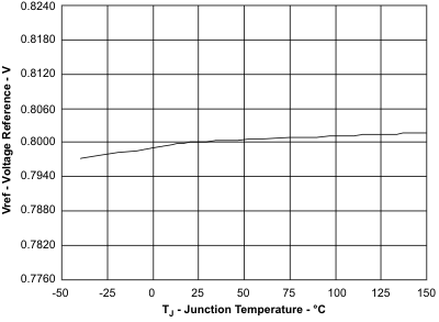 Figure 4. Voltage Reference vs Junction Temperature
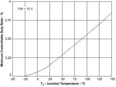 Figure 6. Minimum Controllable Duty Ratio vs
 Junction Temperature
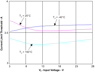 Figure 8. Current Limit Threshold vs Input Voltage
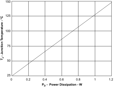 Figure 10. Maximum Power Dissipation vs
 Junction Temperature