SLUS973A October 2009 – November 2016 TPS54290 , TPS54291 , TPS54292
PRODUCTION DATA.
- 1 Features
- 2 Applications
- 3 Description
- 4 Revision History
- 5 Device Comparison Table
- 6 Pin Configuration and Functions
- 7 Specifications
-
8 Detailed Description
- 8.1 Overview
- 8.2 Functional Block Diagram
- 8.3
Feature Description
- 8.3.1 Voltage Reference
- 8.3.2 Oscillator
- 8.3.3 Input UVLO and Start-Up
- 8.3.4 Enable and Timed Turnon of the Outputs
- 8.3.5 Soft Start
- 8.3.6 Output Voltage Regulation
- 8.3.7 Inductor Selection
- 8.3.8 Maximum Output Capacitance
- 8.3.9 Feedback Loop Compensation
- 8.3.10 Bootstrap for N-Channel MOSFET
- 8.3.11 Output Overload Protection
- 8.3.12 Operating Near Maximum Duty Cycle
- 8.3.13 Dual-Supply Operation
- 8.3.14 Bypassing and Filtering
- 8.4 Device Functional Modes
-
9 Application and Implementation
- 9.1 Application Information
- 9.2
Typical Applications
- 9.2.1
TPS54291 Design Example
- 9.2.1.1 Design Requirements
- 9.2.1.2
Detailed Design Procedure
- 9.2.1.2.1 Duty Cycle Estimation
- 9.2.1.2.2 Inductor Selection
- 9.2.1.2.3 Output Capacitor Selection
- 9.2.1.2.4 Input Capacitor Selection
- 9.2.1.2.5 Feedback
- 9.2.1.2.6 Compensation Components
- 9.2.1.2.7 Compensation Gain Setting Resistor
- 9.2.1.2.8 Compensation Integrator Capacitor
- 9.2.1.2.9 Bootstrap Capacitor
- 9.2.1.2.10 Power Dissipation
- 9.2.1.3 Application Curves
- 9.2.2 TPS54290 Cascaded Design Example
- 9.2.1
TPS54291 Design Example
- 10Power Supply Recommendations
- 11Layout
- 12Device and Documentation Support
- 13Mechanical, Packaging, and Orderable Information
Package Options
Mechanical Data (Package|Pins)
- PWP|16
Thermal pad, mechanical data (Package|Pins)
- PWP|16
Orderable Information
1 Features
- 4.5-V to 18-V Input Range
- Output Voltage Range 0.8 V to DMAX × VIN
- Fully Integrated Dual Buck: 1.5 A and 2.5 A
- Three Fixed Switching Frequency Versions:
- TPS54290: 300 kHz
- TPS54291: 600 kHz
- TPS54292: 1.2 MHz
- Integrated UVLO
- 0.8 VREF With 1% Accuracy (0°C to 85°C)
- Internal Soft Start:
- TPS54290: 5.2 ms
- TPS54291: 2.6 ms
- TPS54292: 1.3 ms
- Dual PWM Outputs 180° Out-of-Phase
- Dedicated Enable for Each Channel
- Current Mode Control for Simplified Compensation
- External Compensation
- Pulse-by-Pulse Overcurrent Protection,
2.2-A and 3.8-A Overcurrent Limit - Integrated Bootstrap Switch
- Thermal Shutdown Protection at 145°C
- 16-Pin PowerPAD™ HTSSOP Package
2 Applications
- Set-Top Boxes
- Digital TVs
- Power for DSP
- Consumer Electronics
3 Description
The TPS54290, TPS54291, and TPS54292 devices are dual-output, fully synchronous buck converters capable of supporting applications with a minimal number of external components. It operates from a 4.5-V to 18-V input supply voltage, and supports output voltages as low as 0.8 V and as high as 90% of the input voltage.
Both high-side and low-side MOSFETs are integrated to provide fully synchronous conversion with higher efficiency. Channel 1 can provide up to 1.5 A of continuous current. Meanwhile, Channel 2 supports up to 2.5 A.
Current mode control simplifies the compensation. The external compensation adds flexibility for the user to choose different type of output capacitors.
180° out-of-phase operation reduces the ripple current through the input capacitor, providing the benefit of reducing input capacitance, alleviating EMI and increasing capacitor life.
Device Information(1)
| PART NUMBER | PACKAGE | BODY SIZE (NOM) |
|---|---|---|
| TPS54290 TPS54291 TPS54292 |
HTSSOP (16) | 5.00 mm × 4.40 mm |
- For all available packages, see the orderable addendum at the end of the data sheet.
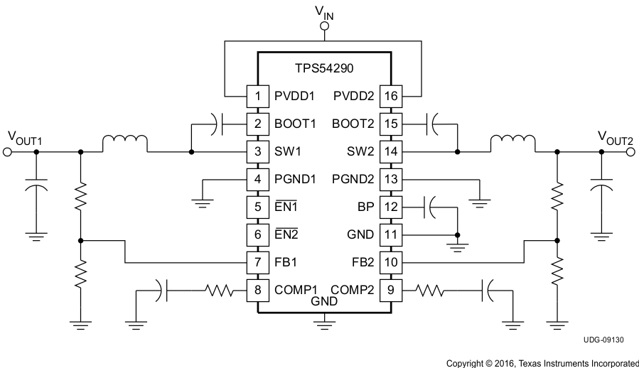
Simplified Schematic
