SLVSDG6B May 2016 – April 2021 TPS54302
PRODUCTION DATA
- 1 Features
- 2 Applications
- 3 Description
- 4 Revision History
- 5 Pin Configuration and Functions
- 6 Specifications
-
7 Detailed Description
- 7.1 Overview
- 7.2 Functional Block Diagram
- 7.3
Feature Description
- 7.3.1 Fixed-Frequency PWM Control
- 7.3.2 Pulse Skip Mode
- 7.3.3 Error Amplifier
- 7.3.4 Slope Compensation and Output Current
- 7.3.5 Enable and Adjusting Undervoltage Lockout
- 7.3.6 Safe Startup into Pre-Biased Outputs
- 7.3.7 Voltage Reference
- 7.3.8 Adjusting Output Voltage
- 7.3.9 Internal Soft-Start
- 7.3.10 Bootstrap Voltage (BOOT)
- 7.3.11 Overcurrent Protection
- 7.3.12 Spread Spectrum
- 7.3.13 Output Overvoltage Protection (OVP)
- 7.3.14 Thermal Shutdown
- 7.4 Device Functional Modes
- 8 Application and Implementation
- 9 Power Supply Recommendations
- 10Layout
- 11Device and Documentation Support
- 12Mechanical, Packaging, and Orderable Information
Package Options
Refer to the PDF data sheet for device specific package drawings
Mechanical Data (Package|Pins)
- DDC|6
Thermal pad, mechanical data (Package|Pins)
Orderable Information
8.2.3.1 Input Capacitor Selection
The device requires an input decoupling capacitor and a bulk capacitor is needed depending on the application. A ceramic capacitor over 10 µF is recommended for the decoupling capacitor. An additional 0.1-µF capacitor (C2) from the VIN pin to GND is optional to provide additional high frequency filtering. The capacitor voltage rating must be greater than the maximum input voltage.
Use Equation 4 to calculate the input ripple voltage (ΔVIN).
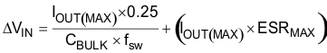
where
- CBULK is the bulk capacitor value.
- fSW is the switching frequency.
- IOUT(MAX) is the maximum loading current.
- ESRMAX is maximum series resistance of the bulk capacitor.
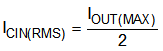
The maximum RMS (root mean square) ripple current must also be checked. For worst case conditions, use Equation 5 to calculate ICIN(RMS).
The actual input-voltage ripple is greatly affected by parasitic associated with the layout and the output impedance of the voltage source. The Section 8.2.2 show the actual input voltage ripple for this circuit which is larger than the calculated value. This measured value is still below the specified input limit of 400 mV. The maximum voltage across the input capacitors is VINmax + ΔVIN / 2. The selected bypass capacitor is rated for 35 V and the ripple current capacity is greater than 2 A. Both values provide ample margin. The maximum ratings for voltage and current must not be exceeded under any circumstance.