SLVSDG6B May 2016 – April 2021 TPS54302
PRODUCTION DATA
- 1 Features
- 2 Applications
- 3 Description
- 4 Revision History
- 5 Pin Configuration and Functions
- 6 Specifications
-
7 Detailed Description
- 7.1 Overview
- 7.2 Functional Block Diagram
- 7.3
Feature Description
- 7.3.1 Fixed-Frequency PWM Control
- 7.3.2 Pulse Skip Mode
- 7.3.3 Error Amplifier
- 7.3.4 Slope Compensation and Output Current
- 7.3.5 Enable and Adjusting Undervoltage Lockout
- 7.3.6 Safe Startup into Pre-Biased Outputs
- 7.3.7 Voltage Reference
- 7.3.8 Adjusting Output Voltage
- 7.3.9 Internal Soft-Start
- 7.3.10 Bootstrap Voltage (BOOT)
- 7.3.11 Overcurrent Protection
- 7.3.12 Spread Spectrum
- 7.3.13 Output Overvoltage Protection (OVP)
- 7.3.14 Thermal Shutdown
- 7.4 Device Functional Modes
- 8 Application and Implementation
- 9 Power Supply Recommendations
- 10Layout
- 11Device and Documentation Support
- 12Mechanical, Packaging, and Orderable Information
Package Options
Refer to the PDF data sheet for device specific package drawings
Mechanical Data (Package|Pins)
- DDC|6
Thermal pad, mechanical data (Package|Pins)
Orderable Information
8.2.3.5.2 Output Capacitor Selection
Consider three primary factors when selecting the value of the output capacitor. The output capacitor determines the modulator pole, the output voltage ripple, and how the regulator responds to a large change in load current. The output capacitance must be selected based on the more stringent of these three criteria.
The desired response to a large change in the load current is the first criterion. The output capacitor must supply the load with current when the regulator cannot. This situation occurs if the desired hold-up times are present for the regulator. In this case, the output capacitor must hold the output voltage above a certain level for a specified amount of time after the input power is removed. The regulator is also temporarily unable to supply sufficient output current if a large, fast increase occurs affecting the current requirements of the load, such as a transition from no load to full load. The regulator usually requires two or more clock cycles for the control loop to notice the change in load current and output voltage and to adjust the duty cycle to react to the change. The output capacitor must be sized to supply the extra current to the load until the control loop responds to the load change. The output capacitance must be large enough to supply the difference in current for 2 clock cycles while only allowing a tolerable amount of drop in the output voltage. Use Equation 11 to calculate the minimum required output capacitance.
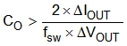
where
- ∆IOUT is the change in output current.
- fSW is the switching frequency of the regulator.
- ∆VOUTb is the allowable change in the output voltage.
For this example, the transient load response is specified as a 5% change in the output voltage, VOUT, for a load step of 1.5 A. For this example, ΔIOUT = 1.5 A and ΔVOUT = 0.05 × 5 = 0.25 V. Using these values results in a minimum capacitance of 30 μF. This value does not consider the ESR of the output capacitor in the output voltage change. For ceramic capacitors, the ESR is usually small enough to ignore in this calculation.
Use Equation 12 to calculate the minimum output capacitance required to meet the output voltage ripple specification. In this case, the maximum output voltage ripple is 30 mV. Under this requirement, Equation 12 yields 10.7 μF.
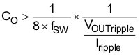
where
- ƒSW is the switching frequency.
- VOUTripple is the maximum allowable output voltage ripple.
- Iripple is the inductor ripple current
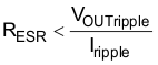
Use Equation 13 to calculate the maximum ESR an output capacitor can have to meet the output-voltage ripple specification. Equation 13 indicates the ESR should be less than 29.2 mΩ. In this case, the ESR of the ceramic capacitor is much smaller than 29.2 mΩ.
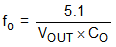
The output capacitor can affect the crossover frequency fo. Considering the loop stability and effect of the internal parasitic parameters, choose the crossover frequency less than 40 kHz without considering the feed forward capacitor. A simple estimation for the crossover frequency without feed forward capacitor C6 is shown in Equation 14, assuming CO has small ESR.
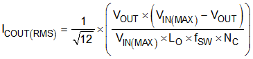
Additional capacitance deratings for aging, temperature, and DC bias should be considered which increases this minimum value. For this example, two 22-uF 25-V, X7R ceramic capacitors are used. Capacitors generally have limits to the amount of ripple current they can handle without failing or producing excess heat. An output capacitor that can support the inductor ripple current must be specified. Some capacitor data sheets specify the RMS value of the maximum ripple current. Use Equation 15 to calculate the RMS ripple current that the output capacitor must support. For this application, Equation 15 yields 296 mA for each capacitor.