SLVSCC4B April 2014 – January 2017 TPS54361-Q1
PRODUCTION DATA.
- 1 Features
- 2 Applications
- 3 Description
- 4 Revision History
- 5 Pin Configuration and Functions
- 6 Specifications
-
7 Detailed Description
- 7.1 Overview
- 7.2 Functional Block Diagram
- 7.3
Feature Description
- 7.3.1 Fixed-Frequency PWM Control
- 7.3.2 Slope Compensation Output Current
- 7.3.3 Pulse-Skip Eco-mode
- 7.3.4 Low Dropout Operation and Bootstrap Voltage (BOOT)
- 7.3.5 Error Amplifier
- 7.3.6 Adjusting the Output Voltage
- 7.3.7 Enable and Adjust Undervoltage Lockout
- 7.3.8 Soft-Start/Tracking Pin (SS/TR)
- 7.3.9 Sequencing
- 7.3.10 Constant Switching Frequency and Timing Resistor (RT/CLK) Pin)
- 7.3.11 Accurate Current-Limit Operation and Maximum Switching Frequency
- 7.3.12 Synchronization to RT/CLK Pin
- 7.3.13 Power Good (PWRGD Pin)
- 7.3.14 Overvoltage Protection
- 7.3.15 Thermal Shutdown
- 7.3.16 Small Signal Model for Loop Response
- 7.3.17 Simple Small Signal Model for Peak Current Mode Control
- 7.3.18 Small Signal Model for Frequency Compensation
- 7.4 Device Functional Modes
-
8 Application and Implementation
- 8.1 Application Information
- 8.2
Typical Application
- 8.2.1 Design Requirements
- 8.2.2
Detailed Design Procedure
- 8.2.2.1 Custom Design with WEBENCH® Tools
- 8.2.2.2 Selecting the Switching Frequency
- 8.2.2.3 Output Inductor Selection (LO)
- 8.2.2.4 Output Capacitor
- 8.2.2.5 Catch Diode
- 8.2.2.6 Input Capacitor
- 8.2.2.7 Slow-Start Capacitor
- 8.2.2.8 Bootstrap Capacitor Selection
- 8.2.2.9 Undervoltage Lockout Set Point
- 8.2.2.10 Output Voltage and Feedback Resistors Selection
- 8.2.2.11 Compensation
- 8.2.2.12 Discontinuous Conduction Mode and Eco-mode Boundary
- 8.2.3 Application Curves
- 9 Power Supply Recommendations
- 10Layout
- 11Device and Documentation Support
- 12Mechanical, Packaging, and Orderable Information
Package Options
Mechanical Data (Package|Pins)
- DPR|10
Thermal pad, mechanical data (Package|Pins)
- DPR|10
Orderable Information
1 Features
- Qualified for Automotive Applications
- AEC-Q100 Qualified With the Following Results:
- Device Temperature Grade 1: –40°C to 125°C Ambient Operating Temperature Range
- Device HBM ESD Classification Level H1C
- Device CDM ESD Classification Level C3B
- High Efficiency at Light Loads with Pulse Skipping Eco-mode™
- 87-mΩ High-Side MOSFET
- 152-μA Operating Quiescent Current and
2-μA Shutdown Current - 100-kHz to 2.5-MHz Adjustable Switching Frequency
- Synchronizes to External Clock
- Low Dropout at Light Loads with Integrated BOOT Recharge FET
- Adjustable UVLO Voltage and Hysteresis
- UV and OV Power Good Output
- Adjustable Soft-Start and Sequencing
- 0.8-V 1% Internal Voltage Reference
- 10-Pin WSON with Thermal Pad Package
- –40°C to 150°C TJ Operating Range
- Create a Custom Design using the TPS54361-Q1 with the WEBENCH® Power Designer
2 Applications
3 Description
The TPS54361-Q1 device is a 60-V, 3.5-A, step down regulator with an integrated high side MOSFET. The device survives load dump pulses up to 65 V per ISO 7637. Current mode control provides simple external compensation and flexible component selection. A low ripple pulse skip mode and supply current of 152-µA enables high efficiency at light loads. Shutdown supply current is reduced to 2 μA when the enable pin is pulled low.
Undervoltage lockout is internally set at 4.3 V but can increase using an external resistor divider at the enable pin. The output voltage startup ramp is controlled by the soft start pin that can also be configured for sequencing/tracking. An open-drain power-good signal indicates the output is within 93% to 106% of the nominal voltage.
A wide adjustable switching-frequency range allows for optimization of either efficiency or external component size. Cycle-by-cycle current-limit, frequency foldback and thermal shutdown protects internal and external components during an overload condition.
The TPS54361-Q1 device is available in a 10-pin
4 mm × 4 mm WSON exposed thermal pad package.
Device Information(1)
| DEVICE NAME | PACKAGE | BODY SIZE |
|---|---|---|
| TPS54361-Q1 | WSON (10) | 4.00 mm × 4.00 mm |
- For all available packages, see the orderable addendum at the end of the data sheet.
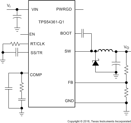
Simplified Schematic

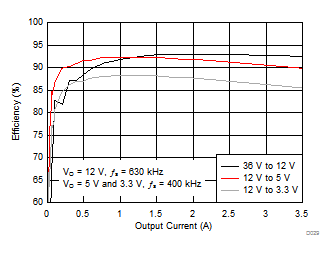
Efficiency vs Load Current
