SLVSDV8 July 2017 TPS54424
PRODUCTION DATA.
- 1 Features
- 2 Applications
- 3 Description
- 4 Revision History
- 5 Pin Configuration and Functions
- 6 Specifications
-
7 Detailed Description
- 7.1 Overview
- 7.2 Functional Block Diagram
- 7.3
Feature Description
- 7.3.1 Fixed Frequency PWM Control
- 7.3.2 Continuous Conduction Mode Operation (CCM)
- 7.3.3 VIN Pins and VIN UVLO
- 7.3.4 Voltage Reference and Adjusting the Output Voltage
- 7.3.5 Error Amplifier
- 7.3.6 Enable and Adjustable UVLO
- 7.3.7 Soft Start and Tracking
- 7.3.8 Safe Start-up into Pre-Biased Outputs
- 7.3.9 Power Good
- 7.3.10 Sequencing (SS/TRK)
- 7.3.11 Adjustable Switching Frequency (RT Mode)
- 7.3.12 Synchronization (CLK Mode)
- 7.3.13 Bootstrap Voltage and 100% Duty Cycle Operation (BOOT)
- 7.3.14 Output Overvoltage Protection (OVP)
- 7.3.15 Overcurrent Protection
- 7.4 Device Functional Modes
-
8 Application and Implementation
- 8.1 Application Information
- 8.2
Typical Application
- 8.2.1 Design Requirements
- 8.2.2
Detailed Design Procedure
- 8.2.2.1 Custom Design With WEBENCH® Tools
- 8.2.2.2 Switching Frequency
- 8.2.2.3 Output Inductor Selection
- 8.2.2.4 Output Capacitor
- 8.2.2.5 Input Capacitor
- 8.2.2.6 Output Voltage Resistors Selection
- 8.2.2.7 Soft-start Capacitor Selection
- 8.2.2.8 Undervoltage Lockout Set Point
- 8.2.2.9 Bootstrap Capacitor Selection
- 8.2.2.10 PGOOD Pull-up Resistor
- 8.2.2.11 Compensation
- 8.2.3 Application Curves
- 9 Power Supply Recommendations
- 10Layout
- 11Device and Documentation Support
- 12Mechanical, Packaging, and Orderable Information
Package Options
Refer to the PDF data sheet for device specific package drawings
Mechanical Data (Package|Pins)
- RNV|18
Thermal pad, mechanical data (Package|Pins)
Orderable Information
7.3.4 Voltage Reference and Adjusting the Output Voltage
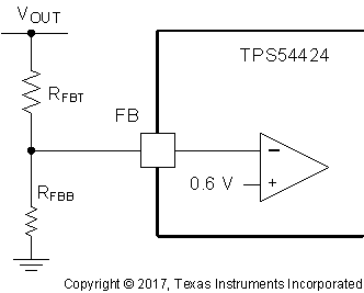
The voltage reference system produces a precise ±0.85%, 0.6 V voltage reference over temperature by scaling the output of a temperature stable band gap circuit. The output voltage is set with a resistor divider from the output (VOUT) to the FB pin shown in Figure 26. It is recommended to use 1% tolerance or better divider resistors. Start with a fixed value for the bottom resistor in the divider, typically 10 kΩ, then use Equation 1 to calculate the top resistor in the divider. To improve efficiency at light loads consider using larger value resistors. If the values are too high the regulator is more susceptible to noise and voltage errors from the FB input current are noticeable. The minimum output voltage and maximum output voltage can be limited by the minimum on time of the high side MOSFET and bootstrap voltage (BOOT-SW voltage) respectively.
 Figure 26. FB Resistor Divider