SLUSCK1C July 2016 – June 2018 TPS546C20A
PRODUCTION DATA.
- 1 Features
- 2 Applications
- 3 Description
- 4 Revision History
- 5 Pin Configuration and Functions
- 6 Specifications
-
7 Detailed Description
- 7.1 Overview
- 7.2 Functional Block Diagram
- 7.3
Feature Description
- 7.3.1 2-Phase Application
- 7.3.2 Linear Regulators BP3 and BP6
- 7.3.3 Input Undervoltage Lockout (UVLO)
- 7.3.4 Turnon and Turnoff Delay and Sequencing
- 7.3.5 Voltage Reference
- 7.3.6 Differential Remote Sense and Compensation
- 7.3.7 Set Output Voltage and Adaptive Voltage Scaling (AVS)
- 7.3.8 Reset VOUT
- 7.3.9 Switching Frequency and Synchronization
- 7.3.10 Current Sharing
- 7.3.11 Soft-Start Time and TON_RISE Command
- 7.3.12 Prebiased Output Start-Up
- 7.3.13 Soft-Stop time and TOFF_FALL Command
- 7.3.14 Output Current Telemetry and Low-Side MOSFET Overcurrent Protection
- 7.3.15 High-Side MOSFET Short-Circuit Protection
- 7.3.16 Die Temperature Telemetry and Overtemperature Protection
- 7.3.17 Output Voltage Telemetry and Over-/Under-voltage Protection
- 7.3.18 TON_MAX Fault
- 7.3.19 Power Good (PGOOD) Indicator
- 7.3.20 Fault Protection Responses
- 7.3.21 Switching Node
- 7.3.22 PMBus General Description
- 7.3.23 PMBus Address
- 7.3.24 PMBus Connections
- 7.3.25 Auto ARA (Alert Response Address) Response
- 7.4 Device Functional Modes
- 7.5 Programming
- 7.6
Register Maps
- 7.6.1 OPERATION (01h)
- 7.6.2 ON_OFF_CONFIG (02h)
- 7.6.3 CLEAR_FAULTS (03h)
- 7.6.4 WRITE_PROTECT (10h)
- 7.6.5 STORE_DEFAULT_ALL (11h)
- 7.6.6 RESTORE_DEFAULT_ALL (12h)
- 7.6.7 STORE_USER_ALL (11h)
- 7.6.8 RESTORE_USER_ALL (12h)
- 7.6.9 CAPABILITY (19h)
- 7.6.10 SMBALERT_MASK (1Bh)
- 7.6.11 VOUT_MODE (20h)
- 7.6.12 VOUT_COMMAND (21h)
- 7.6.13 VOUT_MAX (24h)
- 7.6.14 VOUT_TRANSITION_RATE (27h)
- 7.6.15 VOUT_SCALE_LOOP (29h)
- 7.6.16 VOUT_MIN (2Bh)
- 7.6.17 VIN_ON (35h)
- 7.6.18 VIN_OFF (36h)
- 7.6.19 IOUT_CAL_OFFSET (39h)
- 7.6.20 VOUT_OV_FAULT_RESPONSE (41h)
- 7.6.21 VOUT_UV_FAULT_RESPONSE (45h)
- 7.6.22 IOUT_OC_FAULT_LIMIT (46h)
- 7.6.23 IOUT_OC_FAULT_RESPONSE (47h)
- 7.6.24 IOUT_OC_WARN_LIMIT (4Ah)
- 7.6.25 OT_FAULT_LIMIT (4Fh)
- 7.6.26 OT_FAULT_RESPONSE (50h)
- 7.6.27 OT_WARN_LIMIT (51h)
- 7.6.28 TON_DELAY (60h)
- 7.6.29 TON_RISE (61h)
- 7.6.30 TON_MAX_FAULT_LIMIT (62h)
- 7.6.31 TON_MAX_FAULT_RESPONSE (63h)
- 7.6.32 TOFF_DELAY (64h)
- 7.6.33 TOFF_FALL (65h)
- 7.6.34 STATUS_BYTE (78h)
- 7.6.35 STATUS_WORD (79h)
- 7.6.36 STATUS_VOUT (7Ah)
- 7.6.37 STATUS_IOUT (7Bh)
- 7.6.38 STATUS_INPUT (7Ch)
- 7.6.39 STATUS_TEMPERATURE (7Dh)
- 7.6.40 STATUS_CML (7Eh)
- 7.6.41 STATUS_MFR_SPECIFIC (80h)
- 7.6.42 READ_VOUT (8Bh)
- 7.6.43 READ_IOUT (8Ch)
- 7.6.44 READ_TEMPERATURE_1 (8Dh)
- 7.6.45 PMBUS_REVISION (98h)
- 7.6.46 IC_DEVICE_ID (ADh)
- 7.6.47 IC_DEVICE_REV (AEh)
- 7.6.48 MFR_SPECIFIC_00 (D0h)
- 7.6.49 VREF_TRIM (MFR_SPECIFIC_04) (D4h)
- 7.6.50 STEP_VREF_MARGIN_HIGH (MFR_SPECIFIC_05) (D5h)
- 7.6.51 STEP_VREF_MARGIN_LOW (MFR_SPECIFIC_06) (D6h)
- 7.6.52 PCT_OV_UV_WRN_FLT_LIMITS (MFR_SPECIFIC_07) (D7h)
- 7.6.53
OPTIONS (MFR_SPECIFIC_21) (E5h)
- 7.6.53.1 DIS_NEGILIM Bit
- 7.6.53.2 EN_RESET_B Bit
- 7.6.53.3 EN_ADC_CNTL Bit
- 7.6.53.4 VSM Bit
- 7.6.53.5 DLO Bit
- 7.6.53.6 AVG_PROG[1:0] Bits
- 7.6.53.7 EN_AUTO_ARA Bit
- 7.6.53.8 READ_VOUT_RANGE[1:0] Bits
- 7.6.53.9 EN_DRV_IV_VSEL Bit
- 7.6.53.10 RST_VOUT_oSD Bit
- 7.6.53.11 DIS_VSEL Bit
- 7.6.53.12 RSMLO_VAL Bit
- 7.6.53.13 RSMHI_VAL Bit
- 7.6.54 MISC_CONFIG_OPTIONS (MFR_SPECIFIC_32) (F0h)
-
8 Application and Implementation
- 8.1 Application Information
- 8.2
Typical Application
- 8.2.1
4.5-V to 18-V Input, 1-V Typical Output, 35-A Converter
- 8.2.1.1 Design Requirements
- 8.2.1.2
Detailed Design Procedure
- 8.2.1.2.1 Custom Design With WEBENCH® Tools
- 8.2.1.2.2 Switching Frequency Selection
- 8.2.1.2.3 Inductor Selection
- 8.2.1.2.4 Output Capacitor Selection
- 8.2.1.2.5 Output Voltage Deviation During Load Transient
- 8.2.1.2.6 Output Voltage Ripple
- 8.2.1.2.7 Input Capacitor Selection
- 8.2.1.2.8 AVIN, BP6, BP3 Bypass Capacitor
- 8.2.1.2.9 Bootstrap Capacitor Selection
- 8.2.1.2.10 R-C Snubber
- 8.2.1.2.11 Output Voltage Setting and Frequency Compensation Selection
- 8.2.1.2.12 Key PMBus Parameter Selection
- 8.2.1.2.13 Enable, UVLO
- 8.2.1.2.14 Soft-Start Time
- 8.2.1.2.15 Overcurrent Threshold and Response
- 8.2.1.3 Application Curves
- 8.2.1
4.5-V to 18-V Input, 1-V Typical Output, 35-A Converter
- 9 Power Supply Recommendations
- 10Layout
- 11Device and Documentation Support
- 12Mechanical, Packaging, and Orderable Information
Package Options
Refer to the PDF data sheet for device specific package drawings
Mechanical Data (Package|Pins)
- RVF|40
Thermal pad, mechanical data (Package|Pins)
- RVF|40
Orderable Information
7.3.16 Die Temperature Telemetry and Overtemperature Protection
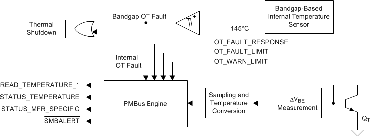
An internal temperature sensor based off the bandgap reference protects the devices from thermal runaway. The internal thermal shutdown threshold, TSD, is fixed at 145°C (typical). When the devices sense a temperature above TSD, an otf_bg bit in the STATUS_MFR_SPECIFIC command is flagged, and power conversion stops until the sensed junction temperature decreases by the amount of the thermal shutdown hysteresis, THYST (20°C typical). The SMBALERT signal is triggered if it is not masked.
The devices also provide temperature telemetry and programmable internal overtemperature fault or warning thresholds using measurements from an internal temperature sensor as shown in Figure 33. The temperature-sensor circuit applies two bias currents to an internal diode-connected NPN transistor, and measures ΔVBE to infer the junction temperature of the sensor. The devices then digitize the result and compare it to the user-configured overtemperature fault and warning thresholds. When an internal overtemperature fault (OTF) is detected, power conversion stops until the sensed temperature decreases by 20°C. The READ_TEMPERATURE_1 (8Dh) register is continually updated with the digitized temperature measurement, enabling temperature telemetry. The OT_FAULT_LIMIT (4Fh) and OT_WARN_LIMIT (51h) commands set the overtemperature fault and warning thresholds through the PMBus interface. When an overtemperature event is detected, the device sets the appropriate flags in STATUS_TEMPERATURE (7Dh) command and triggers the SMBALERT signal if it is not masked.
The device response upon internal overtemperature fault can be set to Latch-off, Restart and Ignore in OT_FAULT_RESPONSE. The default response to an over temperature fault is to ignore. Fixed band gap-detected overtemperature (OT) faults are never ignored. The band gap OT faults always respond in a shutdown and attempted restart once the part cools. Table 4 summarizes the fault-response scheme.
 Figure 33. Overtemperature Protection