SLVSES4C September 2019 – June 2021 TPS54J060
PRODUCTION DATA
- 1 Features
- 2 Applications
- 3 Description
- 4 Revision History
- 5 Pin Configuration and Functions
- 6 Specifications
-
7 Detailed Description
- 7.1 Overview
- 7.2 Functional Block Diagram
- 7.3
Feature Description
- 7.3.1 Enable and Internal LDO
- 7.3.2 Split Rail and External LDO
- 7.3.3 Output Voltage Setting
- 7.3.4 Soft Start and Output-Voltage Tracking
- 7.3.5 Frequency and Operation Mode Selection
- 7.3.6 D-CAP3 Control
- 7.3.7 Current Sense and Positive Overcurrent Protection
- 7.3.8 Low-side FET Negative Current Limit
- 7.3.9 Power Good
- 7.3.10 Overvoltage and Undervoltage Protection
- 7.3.11 Out-Of-Bounds Operation (OOB)
- 7.3.12 Output Voltage Discharge
- 7.3.13 UVLO Protection
- 7.3.14 Thermal Shutdown
- 7.4 Device Functional Modes
-
8 Application and Implementation
- 8.1 Application Information
- 8.2
Typical Application
- 8.2.1 Design Requirements
- 8.2.2
Detailed Design Procedure
- 8.2.2.1 Choose the Switching Frequency and Operation Mode (MODE Pin)
- 8.2.2.2 Choose the Output Inductor (L)
- 8.2.2.3 Set the Current Limit (TRIP)
- 8.2.2.4 Choose the Output Capacitors (COUT)
- 8.2.2.5 Choose the Input Capacitors (CIN)
- 8.2.2.6 Feedback Network (FB Pin)
- 8.2.2.7 Soft Start Capacitor (SS/REFIN Pin)
- 8.2.2.8 EN Pin Resistor Divider
- 8.2.2.9 VCC Bypass Capacitor
- 8.2.2.10 BOOT Capacitor
- 8.2.2.11 Series BOOT Resistor and RC Snubber
- 8.2.2.12 PGOOD Pullup Resistor
- 8.2.3 Application Curves
- 9 Power Supply Recommendations
- 10Layout
- 11Device and Documentation Support
- 12Mechanical, Packaging, and Ordering Information
Package Options
Mechanical Data (Package|Pins)
- RPG|14
Thermal pad, mechanical data (Package|Pins)
Orderable Information
8.2.2.2 Choose the Output Inductor (L)
Calculate the inductance value to set the ripple current at approximately 0.3 times the output current using Equation 8. Larger ripple current improves transient response and improves signal-to-noise ratio with the tradeoff of increased steady state output voltage ripple. Smaller ripple current reduces steady state output voltage ripple with the trade off of slower transient response and may increase jitter. The target ripple current must be between 0.6 A and 3 A. Based on the result of Equation 8, a standard inductance value of 1 µH was selected.

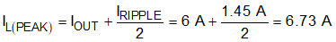
Equation 9 calculates the ripple current with the selected inductance. Equation 10 calculates the peak current in the inductor and the saturation current rating of the inductor should be greater than this. The saturation behavior of the inductor at the peak inductor current at current limit must also be considered when choosing the inductor. Equation 11 calculates the RMS current in the inductor and the heat current rating of the inductor should be greater than this.
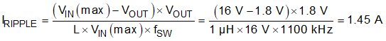

The selected inductance is a CMLE063T-1R0. This has a saturation current rating of 14 A, RMS current rating of 16 A and a DCR of 6.5-mΩ max. This inductor was selected for its low DCR to get high efficiency.