SLVSBV5C June 2014 – September 2021 TPS55340-Q1
PRODUCTION DATA
- 1 Features
- 2 Applications
- 3 Description
- 4 Revision History
- 5 Pin Configuration and Functions
- 6 Specifications
-
7 Detailed Description
- 7.1 Overview
- 7.2 Functional Block Diagram
- 7.3 Feature Description
- 7.4 Device Functional Modes
-
8 Application and Implementation
- 8.1 Application Information
- 8.2
Typical Applications
- 8.2.1
TPS55340-Q1 Boost Converter
- 8.2.1.1 Design Requirements
- 8.2.1.2
Detailed Design Procedure
- 8.2.1.2.1 Custom Design With WEBENCH® Tools
- 8.2.1.2.2 Selecting the Switching Frequency (R4)
- 8.2.1.2.3 Determining the Duty Cycle
- 8.2.1.2.4 Selecting the Inductor (L1)
- 8.2.1.2.5 Computing the Maximum Output Current
- 8.2.1.2.6 Selecting the Output Capacitor (C8 through C10)
- 8.2.1.2.7 Selecting the Input Capacitors (C2 and C7)
- 8.2.1.2.8 Setting the Output Voltage (R1 and R2)
- 8.2.1.2.9 Setting the Soft-Start Time (C7)
- 8.2.1.2.10 Selecting the Schottky Diode (D1)
- 8.2.1.2.11 Compensating the Control Loop (R3, C4, and C5)
- 8.2.1.3 Application Curves
- 8.2.2
TPS55340-Q1 SEPIC Converter
- 8.2.2.1 Design Requirements
- 8.2.2.2
Detailed Design Procedure
- 8.2.2.2.1 Selecting the Switching Frequency (R4)
- 8.2.2.2.2 Duty Cycle
- 8.2.2.2.3 Selecting the Inductor (L1)
- 8.2.2.2.4 Calculating the Maximum Output Current
- 8.2.2.2.5 Selecting the Output Capacitor (C8 Through C10)
- 8.2.2.2.6 Selecting the Series Capacitor (C6)
- 8.2.2.2.7 Selecting the Input Capacitor (C2 and C7)
- 8.2.2.2.8 Selecting the Schottky Diode (D1)
- 8.2.2.2.9 Setting the Output Voltage (R1 and R2)
- 8.2.2.2.10 Setting the Soft-Start Time (C3)
- 8.2.2.2.11 Mosfet Rating Considerations
- 8.2.2.2.12 Compensating the Control Loop (R3 and C4)
- 8.2.2.3 Application Curves
- 8.2.1
TPS55340-Q1 Boost Converter
- 9 Power Supply Recommendations
- 10Layout
- 11Device and Documentation Support
- 12Mechanical, Packaging, and Orderable Information
Package Options
Mechanical Data (Package|Pins)
- RTE|16
Thermal pad, mechanical data (Package|Pins)
- RTE|16
Orderable Information
7.3.6 Slope Compensation
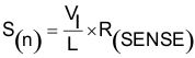
To prevent subharmonic oscillations, the TPS55340-Q1 device uses internal slope compensation. Use Equation 6 to calculate the sensed current slope of boost converter.
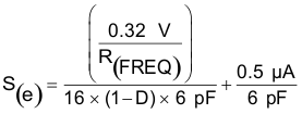
Use Equation 7 to calculate the slope compensation dv/dt.
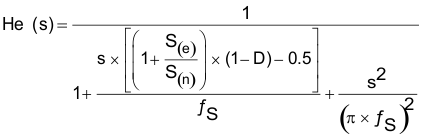
In a converter with current mode control, in addition to the output voltage feedback loop, the inner current loop including the inductor current sampling effect and the slope compensation on the small-signal response must be taken into account as calculated in Equation 8.
where
- R(SENSE) (15 mΩ) is the equivalent current-sense resistor.
- R(FREQ) is the timing resistor used to set frequency.
- D is the duty cycle.
If S(n) << S(e), the converter operates in voltage mode control rather than operating current mode control and Equation 8 is no longer valid.