SLVSBV5C June 2014 – September 2021 TPS55340-Q1
PRODUCTION DATA
- 1 Features
- 2 Applications
- 3 Description
- 4 Revision History
- 5 Pin Configuration and Functions
- 6 Specifications
-
7 Detailed Description
- 7.1 Overview
- 7.2 Functional Block Diagram
- 7.3 Feature Description
- 7.4 Device Functional Modes
-
8 Application and Implementation
- 8.1 Application Information
- 8.2
Typical Applications
- 8.2.1
TPS55340-Q1 Boost Converter
- 8.2.1.1 Design Requirements
- 8.2.1.2
Detailed Design Procedure
- 8.2.1.2.1 Custom Design With WEBENCH® Tools
- 8.2.1.2.2 Selecting the Switching Frequency (R4)
- 8.2.1.2.3 Determining the Duty Cycle
- 8.2.1.2.4 Selecting the Inductor (L1)
- 8.2.1.2.5 Computing the Maximum Output Current
- 8.2.1.2.6 Selecting the Output Capacitor (C8 through C10)
- 8.2.1.2.7 Selecting the Input Capacitors (C2 and C7)
- 8.2.1.2.8 Setting the Output Voltage (R1 and R2)
- 8.2.1.2.9 Setting the Soft-Start Time (C7)
- 8.2.1.2.10 Selecting the Schottky Diode (D1)
- 8.2.1.2.11 Compensating the Control Loop (R3, C4, and C5)
- 8.2.1.3 Application Curves
- 8.2.2
TPS55340-Q1 SEPIC Converter
- 8.2.2.1 Design Requirements
- 8.2.2.2
Detailed Design Procedure
- 8.2.2.2.1 Selecting the Switching Frequency (R4)
- 8.2.2.2.2 Duty Cycle
- 8.2.2.2.3 Selecting the Inductor (L1)
- 8.2.2.2.4 Calculating the Maximum Output Current
- 8.2.2.2.5 Selecting the Output Capacitor (C8 Through C10)
- 8.2.2.2.6 Selecting the Series Capacitor (C6)
- 8.2.2.2.7 Selecting the Input Capacitor (C2 and C7)
- 8.2.2.2.8 Selecting the Schottky Diode (D1)
- 8.2.2.2.9 Setting the Output Voltage (R1 and R2)
- 8.2.2.2.10 Setting the Soft-Start Time (C3)
- 8.2.2.2.11 Mosfet Rating Considerations
- 8.2.2.2.12 Compensating the Control Loop (R3 and C4)
- 8.2.2.3 Application Curves
- 8.2.1
TPS55340-Q1 Boost Converter
- 9 Power Supply Recommendations
- 10Layout
- 11Device and Documentation Support
- 12Mechanical, Packaging, and Orderable Information
Package Options
Mechanical Data (Package|Pins)
- RTE|16
Thermal pad, mechanical data (Package|Pins)
- RTE|16
Orderable Information
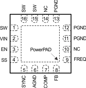
5 Pin Configuration and Functions

TI recommends
connecting NC with AGND.
Figure 5-1 16-Pin QFN With PowerPADRTE
Package(Top View)Table 5-1 Pin Functions
| PIN | DESCRIPTION | |
|---|---|---|
| NAME | NO. | |
| AGND | 6 | Signal ground of the IC |
| COMP | 7 | Output of the transconductance error amplifier. An external RC network connected to this pin compensates the regulator feedback loop. |
| EN | 3 | Enable pin. When the voltage of this pin falls below the enable threshold for more than 1 ms, the IC turns off. |
| FB | 8 | Error amplifier input and feedback pin for positive voltage regulation. Connect the FB pin to the center tap of a resistor divider to program the output voltage. |
| FREQ | 9 | Switching frequency program pin. An external resistor connected between the FREQ pin and the AGND pin sets the switching frequency. |
| NC | 10 | This pin is reserved and must be connected to ground. |
| 14 | ||
| PGND | 11 | Power ground of the IC. The PGND pin is connected to the source of the internal power MOSFET switch. |
| 12 | ||
| 13 | ||
| SS | 4 | Soft-start programming pin. A capacitor between the SS pin and AGND pin programs soft-start timing. |
| SW | 1 | SW is the drain of the internal power MOSFET. Connect the SW pin to the switched side of the boost or SEPIC inductor or the flyback transformer. |
| 15 | ||
| 16 | ||
| SYNC | 5 | Switching frequency synchronization pin. An external clock signal can set the switching frequency between 200 kHz and 1 MHz. If this pin is not used, it must be tied to AGND. |
| VIN | 2 | The input supply pin to the IC. Connect the VIN pin to a supply voltage between 2.9 V and 32 V. The voltage on the VIN pin can be different from the boost power stage input. |
| PowerPAD | The PowerPAD must be soldered to AGND. If possible, use thermal vias to connect the PowerPAD to PCB ground plane layers for improved power dissipation. | |