SLVSBV5C June 2014 – September 2021 TPS55340-Q1
PRODUCTION DATA
- 1 Features
- 2 Applications
- 3 Description
- 4 Revision History
- 5 Pin Configuration and Functions
- 6 Specifications
-
7 Detailed Description
- 7.1 Overview
- 7.2 Functional Block Diagram
- 7.3 Feature Description
- 7.4 Device Functional Modes
-
8 Application and Implementation
- 8.1 Application Information
- 8.2
Typical Applications
- 8.2.1
TPS55340-Q1 Boost Converter
- 8.2.1.1 Design Requirements
- 8.2.1.2
Detailed Design Procedure
- 8.2.1.2.1 Custom Design With WEBENCH® Tools
- 8.2.1.2.2 Selecting the Switching Frequency (R4)
- 8.2.1.2.3 Determining the Duty Cycle
- 8.2.1.2.4 Selecting the Inductor (L1)
- 8.2.1.2.5 Computing the Maximum Output Current
- 8.2.1.2.6 Selecting the Output Capacitor (C8 through C10)
- 8.2.1.2.7 Selecting the Input Capacitors (C2 and C7)
- 8.2.1.2.8 Setting the Output Voltage (R1 and R2)
- 8.2.1.2.9 Setting the Soft-Start Time (C7)
- 8.2.1.2.10 Selecting the Schottky Diode (D1)
- 8.2.1.2.11 Compensating the Control Loop (R3, C4, and C5)
- 8.2.1.3 Application Curves
- 8.2.2
TPS55340-Q1 SEPIC Converter
- 8.2.2.1 Design Requirements
- 8.2.2.2
Detailed Design Procedure
- 8.2.2.2.1 Selecting the Switching Frequency (R4)
- 8.2.2.2.2 Duty Cycle
- 8.2.2.2.3 Selecting the Inductor (L1)
- 8.2.2.2.4 Calculating the Maximum Output Current
- 8.2.2.2.5 Selecting the Output Capacitor (C8 Through C10)
- 8.2.2.2.6 Selecting the Series Capacitor (C6)
- 8.2.2.2.7 Selecting the Input Capacitor (C2 and C7)
- 8.2.2.2.8 Selecting the Schottky Diode (D1)
- 8.2.2.2.9 Setting the Output Voltage (R1 and R2)
- 8.2.2.2.10 Setting the Soft-Start Time (C3)
- 8.2.2.2.11 Mosfet Rating Considerations
- 8.2.2.2.12 Compensating the Control Loop (R3 and C4)
- 8.2.2.3 Application Curves
- 8.2.1
TPS55340-Q1 Boost Converter
- 9 Power Supply Recommendations
- 10Layout
- 11Device and Documentation Support
- 12Mechanical, Packaging, and Orderable Information
Package Options
Mechanical Data (Package|Pins)
- RTE|16
Thermal pad, mechanical data (Package|Pins)
- RTE|16
Orderable Information
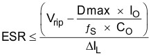
8.2.1.2.6 Selecting the Output Capacitor (C8 through C10)
At least 4.7 µF of ceramic type X5R or X7R capacitance is recommended at the output. This output capacitance was selected to meet the requirements for the output ripple (Vrip) and voltage change during a load transient. The loop is then compensated for the selected output capacitor. The output capacitance must be selected based on the most stringent of these criteria. The output ripple voltage is related to the capacitance and equivalent series resistance (ESR) of the output capacitor. Assuming a capacitor with zero ESR, use Equation 20 to calculate the minimum capacitance required for a given ripple. Using high-ESR capacitors causes additional ripple. Use Equation 21 to calculate the maximum ESR for a specified ripple. ESR ripple can be neglected for ceramic capacitors, but must be considered if tantalum or electrolytic capacitors are used. Use Equation 22 to calculate the minimum ceramic output capacitance required to meet a load transient requirement. Use Equation 23 to calculate the RMS current required by the output capacitor for support.
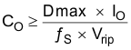
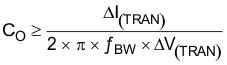
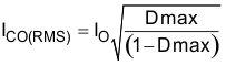
Using Equation 20 for this design, the minimum output capacitance for the specified 120-mV output ripple is 8.8 µF. For a maximum transient voltage change (ΔV(TRAN)) of 960 mV with a 400-mA load transient (ΔI(TRAN)), and a 6-kHz control loop bandwidth (ƒBW) with Equation 22, the minimum output capacitance is calculated as 11.1 µF. The most stringent criterion is the 11.1 µF for the required load transient. Equation 23 calculates a 1.58-A RMS current in the output capacitor. The capacitor must also be properly rated for the desired output voltage.
Care must be taken when evaluating ceramic capacitors that derate under DC bias, aging, and AC signal conditions. For example, larger form factor capacitors (in 1206 size) have self-resonant frequencies in the range of the converter switching frequency. Self resonance significantly decreases the effective capacitance. The DC bias also significantly reduces capacitance. Ceramic capacitors can lose as much as 50% of the capacitance when operated at the rated voltage. Therefore, leave a margin when selecting the capacitor voltage rating to ensure adequate capacitance at the required output voltage. For this example, three 4.7-µF, 50-V 1210 X7R ceramic capacitors are used in parallel, leading to a negligible ESR. Selecting 50-V capacitors instead of 35-V capacitors reduces the effects of DC bias and allows this example circuit to be rated for the maximum output voltage range of the TPS55340-Q1 device.