SLVSBV5C June 2014 – September 2021 TPS55340-Q1
PRODUCTION DATA
- 1 Features
- 2 Applications
- 3 Description
- 4 Revision History
- 5 Pin Configuration and Functions
- 6 Specifications
-
7 Detailed Description
- 7.1 Overview
- 7.2 Functional Block Diagram
- 7.3 Feature Description
- 7.4 Device Functional Modes
-
8 Application and Implementation
- 8.1 Application Information
- 8.2
Typical Applications
- 8.2.1
TPS55340-Q1 Boost Converter
- 8.2.1.1 Design Requirements
- 8.2.1.2
Detailed Design Procedure
- 8.2.1.2.1 Custom Design With WEBENCH® Tools
- 8.2.1.2.2 Selecting the Switching Frequency (R4)
- 8.2.1.2.3 Determining the Duty Cycle
- 8.2.1.2.4 Selecting the Inductor (L1)
- 8.2.1.2.5 Computing the Maximum Output Current
- 8.2.1.2.6 Selecting the Output Capacitor (C8 through C10)
- 8.2.1.2.7 Selecting the Input Capacitors (C2 and C7)
- 8.2.1.2.8 Setting the Output Voltage (R1 and R2)
- 8.2.1.2.9 Setting the Soft-Start Time (C7)
- 8.2.1.2.10 Selecting the Schottky Diode (D1)
- 8.2.1.2.11 Compensating the Control Loop (R3, C4, and C5)
- 8.2.1.3 Application Curves
- 8.2.2
TPS55340-Q1 SEPIC Converter
- 8.2.2.1 Design Requirements
- 8.2.2.2
Detailed Design Procedure
- 8.2.2.2.1 Selecting the Switching Frequency (R4)
- 8.2.2.2.2 Duty Cycle
- 8.2.2.2.3 Selecting the Inductor (L1)
- 8.2.2.2.4 Calculating the Maximum Output Current
- 8.2.2.2.5 Selecting the Output Capacitor (C8 Through C10)
- 8.2.2.2.6 Selecting the Series Capacitor (C6)
- 8.2.2.2.7 Selecting the Input Capacitor (C2 and C7)
- 8.2.2.2.8 Selecting the Schottky Diode (D1)
- 8.2.2.2.9 Setting the Output Voltage (R1 and R2)
- 8.2.2.2.10 Setting the Soft-Start Time (C3)
- 8.2.2.2.11 Mosfet Rating Considerations
- 8.2.2.2.12 Compensating the Control Loop (R3 and C4)
- 8.2.2.3 Application Curves
- 8.2.1
TPS55340-Q1 Boost Converter
- 9 Power Supply Recommendations
- 10Layout
- 11Device and Documentation Support
- 12Mechanical, Packaging, and Orderable Information
Package Options
Mechanical Data (Package|Pins)
- RTE|16
Thermal pad, mechanical data (Package|Pins)
- RTE|16
Orderable Information
7.3.2 Switching Frequency
The switching frequency is set by a resistor (R(FREQ)) connected to the FREQ pin of the TPS55340-Q1 device. The relationship between the resistance of R(FREQ) and frequency is shown in Figure 6-5. Do not leave this pin open. A resistor must always be connected from the FREQ pin to ground for proper operation. Use Equation 1 to calculate the resistor value required for a desired frequency.
For the given resistor value, use Equation 2 to calculate the corresponding frequency.
The TPS55340-Q1 switching frequency can synchronized to an external clock signal that is applied to the SYNC pin. The required logic levels of the external clock are shown in Section 6.5. The recommended duty cycle of the clock is between 10% to 90%. A resistor must be connected from the FREQ pin to ground when the converter is synchronized to the external clock and the external clock frequency must be within ±20% of the corresponding frequency set by the resistor. For example, if the frequency programmed by the FREQ pin resistor is 600 kHz, the external clock signal must be in the range of 480 to 720 kHz.
With a switching frequency below 280 kHz (typical) after the TPS55340-Q1 enters frequency foldback as described in Section 7.3.3, if a load remains when the overcurrent condition is removed, the output may not recover to the set value. For the output to return to the set value, the load must be removed completely or the TPS55340-Q1 power cycled with the EN pin or VIN pin. Select a nominal switching frequency of 350 kHz for quicker recovery from frequency foldback.
When setting the switching frequency higher than 1.2 MHz, TI recommends using an external synchronous clock as the switching frequency to ensure that the pulse-skipping function works at a light load. When using the internal switching frequency above 1.2 MHz, the TPS55340-Q1 device might not pulse skip as described in Section 7.3.3.1. When the pulse-skipping function does not work at light loads, the TPS55340-Q1 device always operates in PWM mode with a minimum ON pulse width. This causes the output voltage to be higher than the set value with the resistor divider at the FB pin. This occurs in minimum duty cycle conditions such as when there is light output load or when the input voltage is close to the set output voltage in a boost topology. In the light load condition, a minimum output load will keep the output voltage at the set value in a boost topology. The required minimum load can be estimated with Equation 3 or Equation 4 using the maximum minimum on time of 107 ns and a parasitic C(SW) capacitance of 150 pF. For example, when boosting 5 V to 12 V with 2.5-MHz switching frequency and a 2-µH inductor, the worst case minimum output load is 36 mA.
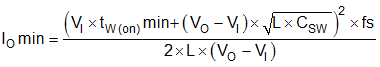 when VO – VI < VI
 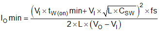 when VO – VI > VI