SLVSBV5C June 2014 – September 2021 TPS55340-Q1
PRODUCTION DATA
- 1 Features
- 2 Applications
- 3 Description
- 4 Revision History
- 5 Pin Configuration and Functions
- 6 Specifications
-
7 Detailed Description
- 7.1 Overview
- 7.2 Functional Block Diagram
- 7.3 Feature Description
- 7.4 Device Functional Modes
-
8 Application and Implementation
- 8.1 Application Information
- 8.2
Typical Applications
- 8.2.1
TPS55340-Q1 Boost Converter
- 8.2.1.1 Design Requirements
- 8.2.1.2
Detailed Design Procedure
- 8.2.1.2.1 Custom Design With WEBENCH® Tools
- 8.2.1.2.2 Selecting the Switching Frequency (R4)
- 8.2.1.2.3 Determining the Duty Cycle
- 8.2.1.2.4 Selecting the Inductor (L1)
- 8.2.1.2.5 Computing the Maximum Output Current
- 8.2.1.2.6 Selecting the Output Capacitor (C8 through C10)
- 8.2.1.2.7 Selecting the Input Capacitors (C2 and C7)
- 8.2.1.2.8 Setting the Output Voltage (R1 and R2)
- 8.2.1.2.9 Setting the Soft-Start Time (C7)
- 8.2.1.2.10 Selecting the Schottky Diode (D1)
- 8.2.1.2.11 Compensating the Control Loop (R3, C4, and C5)
- 8.2.1.3 Application Curves
- 8.2.2
TPS55340-Q1 SEPIC Converter
- 8.2.2.1 Design Requirements
- 8.2.2.2
Detailed Design Procedure
- 8.2.2.2.1 Selecting the Switching Frequency (R4)
- 8.2.2.2.2 Duty Cycle
- 8.2.2.2.3 Selecting the Inductor (L1)
- 8.2.2.2.4 Calculating the Maximum Output Current
- 8.2.2.2.5 Selecting the Output Capacitor (C8 Through C10)
- 8.2.2.2.6 Selecting the Series Capacitor (C6)
- 8.2.2.2.7 Selecting the Input Capacitor (C2 and C7)
- 8.2.2.2.8 Selecting the Schottky Diode (D1)
- 8.2.2.2.9 Setting the Output Voltage (R1 and R2)
- 8.2.2.2.10 Setting the Soft-Start Time (C3)
- 8.2.2.2.11 Mosfet Rating Considerations
- 8.2.2.2.12 Compensating the Control Loop (R3 and C4)
- 8.2.2.3 Application Curves
- 8.2.1
TPS55340-Q1 Boost Converter
- 9 Power Supply Recommendations
- 10Layout
- 11Device and Documentation Support
- 12Mechanical, Packaging, and Orderable Information
Package Options
Mechanical Data (Package|Pins)
- RTE|16
Thermal pad, mechanical data (Package|Pins)
- RTE|16
Orderable Information
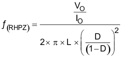
8.2.2.2.12 Compensating the Control Loop (R3 and C4)
This design was compensated by measuring the frequency response of the power stage at the lowest input voltage of 6 V and choosing the components for the desired bandwidth. The lowest right-half plane zero (ƒ(RHPZ)) is calculated with Equation 54 to be 36.7 kHz. When using the recommendation of limiting the bandwidth to 1/3 of ƒ(RHPZ) or less, the recommended maximum bandwidth is 12.2 kHz.
This design also uses only one pole and one zero. To achieve approximately 60 degrees of phase margin, the power stage phase must be no lower than approximately –120 degrees at the desired bandwidth. To ensure a stable design, R3 was initially set to 1 kΩ and C4 was set to 1 µF. Figure 8-11 shows the measurement of the power stage. At 7 kHz, the power stage has a gain of 19.52 dB and phase of –118.1 degrees.
 Figure 8-11 SEPIC Power Stage Gain and Phase
Because no changes occur in the transconductance amplifier, the equations used to calculate the external compensation components in a boost design can be used in the SEPIC design. Using the maximum gm(ea) from the electrical specification of 440 µmho, Equation 40 calculates the nearest standard value of R3 to be 2.37 kΩ. Using Equation 41, C4 is calculated to the nearest standard value of 0.1 µF.