SLVSBV5C June 2014 – September 2021 TPS55340-Q1
PRODUCTION DATA
- 1 Features
- 2 Applications
- 3 Description
- 4 Revision History
- 5 Pin Configuration and Functions
- 6 Specifications
-
7 Detailed Description
- 7.1 Overview
- 7.2 Functional Block Diagram
- 7.3 Feature Description
- 7.4 Device Functional Modes
-
8 Application and Implementation
- 8.1 Application Information
- 8.2
Typical Applications
- 8.2.1
TPS55340-Q1 Boost Converter
- 8.2.1.1 Design Requirements
- 8.2.1.2
Detailed Design Procedure
- 8.2.1.2.1 Custom Design With WEBENCH® Tools
- 8.2.1.2.2 Selecting the Switching Frequency (R4)
- 8.2.1.2.3 Determining the Duty Cycle
- 8.2.1.2.4 Selecting the Inductor (L1)
- 8.2.1.2.5 Computing the Maximum Output Current
- 8.2.1.2.6 Selecting the Output Capacitor (C8 through C10)
- 8.2.1.2.7 Selecting the Input Capacitors (C2 and C7)
- 8.2.1.2.8 Setting the Output Voltage (R1 and R2)
- 8.2.1.2.9 Setting the Soft-Start Time (C7)
- 8.2.1.2.10 Selecting the Schottky Diode (D1)
- 8.2.1.2.11 Compensating the Control Loop (R3, C4, and C5)
- 8.2.1.3 Application Curves
- 8.2.2
TPS55340-Q1 SEPIC Converter
- 8.2.2.1 Design Requirements
- 8.2.2.2
Detailed Design Procedure
- 8.2.2.2.1 Selecting the Switching Frequency (R4)
- 8.2.2.2.2 Duty Cycle
- 8.2.2.2.3 Selecting the Inductor (L1)
- 8.2.2.2.4 Calculating the Maximum Output Current
- 8.2.2.2.5 Selecting the Output Capacitor (C8 Through C10)
- 8.2.2.2.6 Selecting the Series Capacitor (C6)
- 8.2.2.2.7 Selecting the Input Capacitor (C2 and C7)
- 8.2.2.2.8 Selecting the Schottky Diode (D1)
- 8.2.2.2.9 Setting the Output Voltage (R1 and R2)
- 8.2.2.2.10 Setting the Soft-Start Time (C3)
- 8.2.2.2.11 Mosfet Rating Considerations
- 8.2.2.2.12 Compensating the Control Loop (R3 and C4)
- 8.2.2.3 Application Curves
- 8.2.1
TPS55340-Q1 Boost Converter
- 9 Power Supply Recommendations
- 10Layout
- 11Device and Documentation Support
- 12Mechanical, Packaging, and Orderable Information
Package Options
Mechanical Data (Package|Pins)
- RTE|16
Thermal pad, mechanical data (Package|Pins)
- RTE|16
Orderable Information
8.2.1.2.4 Selecting the Inductor (L1)
The selection of the inductor affects steady state operation as well as transient behavior and loop stability. Because of these factors, the inductor is the most important component in the power regulator design. There are three important inductor specifications: inductor value, DC resistance, and saturation current. Considering inductor value alone is not enough. Inductor values can have ±20% tolerance with no current bias. When the inductor current approaches saturation level, the effective inductance can fall to a fraction of the zero current value.
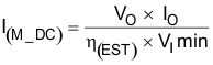
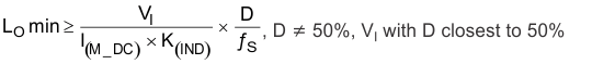
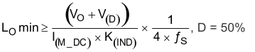
The minimum value of the inductor must meet the inductor current ripple (ΔIL) requirement at worst case. In a boost converter, the maximum inductor-current ripple occurs at 50% duty cycle. For applications where duty cycle is always smaller or larger than 50%, use Equation 14 to calculate the minimum inductance with the duty cycle as close to 50% as possible and the corresponding input voltage. For applications that must operate with 50% duty cycle when input voltage is somewhere between the minimum and the maximum input voltage, use Equation 15. K(IND) is a coefficient that represents the amount of inductor ripple current relative to the maximum input current (I(M_DC) = ILavg). Use Equation 13 to calculate the maximum input current with an estimated efficiency based on similar applications (η(EST)). The inductor ripple current is filtered by the output capacitor. Therefore, choosing high inductor ripple currents impacts the selection of the output capacitor because the output capacitor must have a ripple-current rating equal to or greater than the inductor ripple current. In general, the inductor ripple value (K(IND)) is at the discretion of the designer. However, the following guidelines can be used to select the value for K(IND).
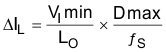
For CCM operation, TI recommends to use K(IND) values in the range of 0.2 to 0.4. Selecting a value for K(IND) that is closer to 0.2 results in a larger inductance value, maximizes the potential output current of the converter, and minimizes electromagnetic interference (EMI). Selecting a value for K(IND) that is closer to 0.4 results in a smaller inductance value, a physically smaller inductor, and improved transient response. However, a K(IND) value close to 0.4 can result in potentially worse EMI and lower efficiency. Using an inductor with a smaller inductance value can result in the converter operating in DCM. Operating in DCM reduces the maximum output current of the boost converter, causes larger input voltage and output voltage ripple, and reduces efficiency. For this design, a value of 0.3 for K(IND) was selected along with a conservative efficiency estimate of 85% with the minimum input voltage and maximum output current. Use Equation 14 to calculate the minimum output inductance with the maximum input voltage because this equation corresponds to duty cycle closest to 50%. The maximum input current is estimated at 4.52 A and the minimum inductance is 7.53 µH. A standard value of 10 µH is selected.
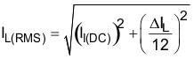
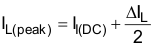
After selecting the inductance, the required current ratings can be calculated. Use Equation 16 to calculate the ripple using the selected inductance. At a minimum input voltage, the inductor has the largest current ripple, therefore, the minimum VI is used in Equation 16. Use Equation 17 and Equation 18 to calculate the root mean square (RMS) and peak inductor current. For this design, the current ripple is 663 mA, the RMS inductor current is 4.52 A, and the peak inductor current is 4.85 A. TI recommends that the peak inductor current rating of the selected inductor be 20% higher to account for transients during power up, faults, or transient load conditions. The most conservative approach is to specify an inductor with a saturation current greater than the maximum peak current limit of the TPS55340-Q1 device. This approach helps to avoid saturation of the inductor. The selected inductor for this design was a Würth Elektronik 74437368100. This inductor has a saturation current rating of 12.5 A, RMS current rating of 5.2 A, and typical DCR of 27 mΩ.
The TPS55340-Q1 device has built-in slope compensation to avoid subharmonic oscillation associated with current mode control. If the inductor value is too small, the slope compensation may not be adequate, and the loop can be unstable.