SLUSDL8B December 2019 – April 2021 TPS563202
PRODUCTION DATA
- 1 Features
- 2 Applications
- 3 Description
- 4 Revision History
- 5 Pin Configuration and Functions
- 6 Specifications
- 7 Detailed Description
- 8 Application and Implementation
- 9 Layout
- 10Device and Documentation Support
- 11Mechanical, Packaging, and Orderable Information
Package Options
Mechanical Data (Package|Pins)
- DRL|6
Thermal pad, mechanical data (Package|Pins)
Orderable Information
6.6 Typical Characteristics
VIN = 12 V (unless otherwise noted)
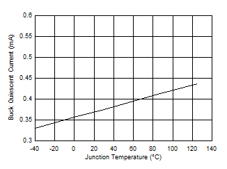 Figure 6-1 Supply Current vs Junction Temperature
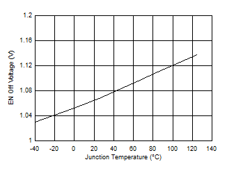 Figure 6-3 EN
Pin EN Off Voltage vs Junction Temperature
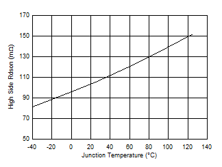 Figure 6-5 High-Side Rds-On vs Junction Temperature
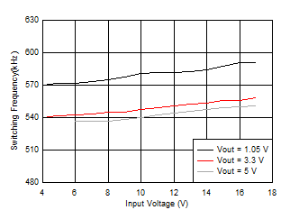 Figure 6-7 Switching Frequency vs Input Voltage
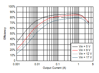 Figure 6-9 VOUT = 0.95 V Efficiency, L = 1.2 µH
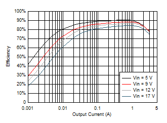 Figure 6-11 VOUT = 1.5 V Efficiency, L = 1.5 µH
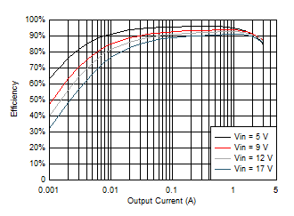 Figure 6-13 VOUT = 3.3 V Efficiency, L = 3.3µH
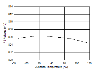 Figure 6-2 FB
Voltage vs Junction Temperature
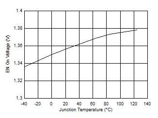 Figure 6-4 EN
Pin EN On Voltage vs Junction Temperature
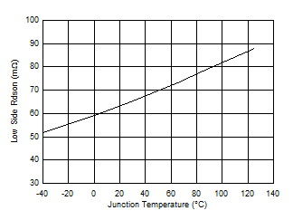 Figure 6-6 Low-Side Rds-On vs Junction Temperature
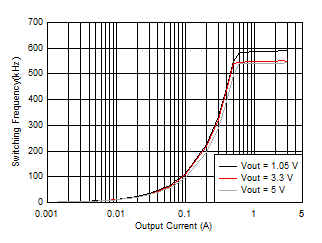 Figure 6-8 Switching Frequency vs Output Current
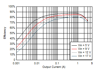 Figure 6-10 VOUT = 1.05 V Efficiency, L = 1.2 µH
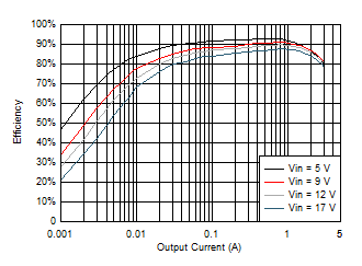 Figure 6-12 VOUT = 1.8 V Efficiency, L = 2.2 µH
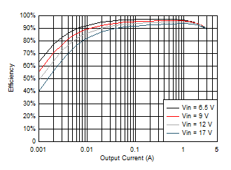 Figure 6-14 VOUT = 5 V Efficiency, L = 4.7µH