SLUSDL8B December   2019  – April 2021 TPS563202

PRODUCTION DATA  

  1. Features
  2. Applications
  3. Description
  4. Revision History
  5. Pin Configuration and Functions
  6. Specifications
    1. 6.1 Absolute Maximum Ratings
    2. 6.2 ESD Ratings
    3. 6.3 Recommended Operating Conditions
    4. 6.4 Thermal Information
    5. 6.5 Electrical Characteristics
    6. 6.6 Typical Characteristics
  7. Detailed Description
    1. 7.1 Overview
    2. 7.2 Functional Block Diagram
    3. 7.3 Feature Description
      1. 7.3.1 Adaptive On-Time Control and PWM Operation
      2. 7.3.2 ECO Mode Control
      3. 7.3.3 Soft Start and Pre-Biased Soft Start
      4. 7.3.4 Current Protection
      5. 7.3.5 Undervoltage Lockout (UVLO) Protection
      6. 7.3.6 Thermal Shutdown
    4. 7.4 Device Functional Modes
      1. 7.4.1 Normal Operation
      2. 7.4.2 Eco-mode Operation
      3. 7.4.3 Standby Operation
  8. Application and Implementation
    1. 8.1 Application Information
    2. 8.2 Typical Application
      1. 8.2.1 Design Requirements
      2. 8.2.2 Detailed Design Procedure
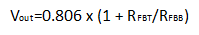
        1. 8.2.2.1 Output Voltage Resistors Selection
        2. 8.2.2.2 Output Filter Selection
        3. 8.2.2.3 Input Capacitor Selection
        4. 8.2.2.4 Bootstrap Capacitor Selection
      3. 8.2.3 Application Curves
  9. Layout
    1. 9.1 Layout Guidelines
    2. 9.2 Layout Example
  10. 10Device and Documentation Support
    1. 10.1 Receiving Notification of Documentation Updates
    2. 10.2 Support Resources
    3. 10.3 Trademarks
    4. 10.4 Electrostatic Discharge Caution
    5. 10.5 Glossary
  11. 11Mechanical, Packaging, and Orderable Information

Package Options

Mechanical Data (Package|Pins)
Thermal pad, mechanical data (Package|Pins)
Orderable Information

Output Voltage Resistors Selection

The output voltage is set with a resistor divider from the output node to the FB pin. TI recommends to use 1% tolerance or better divider resistors. Start by using Equation 2 to calculate VOUT.

To improve efficiency at very light loads consider using larger value resistors, too high of resistance will be more susceptible to noise and voltage errors from the FB input current will be more noticeable.

Equation 2. GUID-CB83FF86-9335-4D35-92EA-8D06763983DB-low.gif