SLUSDX1A September 2020 – August 2021 TPS563211
PRODUCTION DATA
- 1 Features
- 2 Applications
- 3 Description
- 4 Revision History
- 5 Pin Configuration and Functions
- 6 Specifications
-
7 Detailed Description
- 7.1 Overview
- 7.2 Functional Block Diagram
- 7.3
Feature Description
- 7.3.1 Advanced Emulated Current Mode Control
- 7.3.2 Mode Selection and PG/SS Pin Function Configuration
- 7.3.3 Power Good (PG)
- 7.3.4 Soft Start and Pre-Biased Soft Start
- 7.3.5 Output Discharge through PG/SS Pin
- 7.3.6 Precise Enable and Adjusting Undervoltage Lockout
- 7.3.7 Overcurrent Limit and Undervoltage Protection
- 7.3.8 Overvoltage Protection
- 7.3.9 Thermal Shutdown
- 7.4 Device Functional Modes
- 8 Application and Implementation
- 9 Power Supply Recommendations
- 10Layout
- 11Device and Documentation Support
- 12Mechanical, Packaging, and Orderable Information
Package Options
Mechanical Data (Package|Pins)
- DRL|8
Thermal pad, mechanical data (Package|Pins)
Orderable Information
5 Pin Configuration and Functions
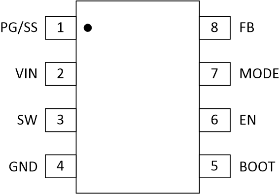
 Figure 5-1 8-Pin SOT583 DRL Package (Top
View)
Figure 5-1 8-Pin SOT583 DRL Package (Top
View)Table 5-1 Pin Functions
| PIN | I/O(1) | DESCRIPTION | |
|---|---|---|---|
| NAME | NO. | ||
| PG/SS | 1 | I/O | This pin can be selected as Power-Good function or Soft-Start
function, depending on device MODE pin configuration.
|
| VIN | 2 | P | Input voltage supply pin for the control circuitry. Connect the input decoupling capacitors between VIN and GND. |
| SW | 3 | P | Switch node terminal. Connect the output inductor to this pin. |
| GND | 4 | G | GND terminal for the controller circuit and the internal circuitry |
| BOOT | 5 | P | Supply input for the high-side MOSFET gate drive circuit. Connect a 0.1-µF capacitor between BOOT and SW pins. |
| EN | 6 | I/O | Enable input control. Driving EN high or leaving this pin floating enables the converter. An external resistor divider can be used to imply an adjustable VIN UVLO function. |
| MODE | 7 | I/O | Device operation mode in light load (Eco-mode operation or FCCM operation) and pin 1 function (Power-Good pin or Soft-Start pin) selection pin. Connect a resistor from MODE to GND to configure the device according to Table 7-1. |
| FB | 8 | I | Converter feedback input. Connect to output voltage with feedback resistor divider. |
(1) I = Input, O = Output, I/O =
Input or Output, G = Ground, P = Power