SLUSDX1A September 2020 – August 2021 TPS563211
PRODUCTION DATA
- 1 Features
- 2 Applications
- 3 Description
- 4 Revision History
- 5 Pin Configuration and Functions
- 6 Specifications
-
7 Detailed Description
- 7.1 Overview
- 7.2 Functional Block Diagram
- 7.3
Feature Description
- 7.3.1 Advanced Emulated Current Mode Control
- 7.3.2 Mode Selection and PG/SS Pin Function Configuration
- 7.3.3 Power Good (PG)
- 7.3.4 Soft Start and Pre-Biased Soft Start
- 7.3.5 Output Discharge through PG/SS Pin
- 7.3.6 Precise Enable and Adjusting Undervoltage Lockout
- 7.3.7 Overcurrent Limit and Undervoltage Protection
- 7.3.8 Overvoltage Protection
- 7.3.9 Thermal Shutdown
- 7.4 Device Functional Modes
- 8 Application and Implementation
- 9 Power Supply Recommendations
- 10Layout
- 11Device and Documentation Support
- 12Mechanical, Packaging, and Orderable Information
Package Options
Mechanical Data (Package|Pins)
- DRL|8
Thermal pad, mechanical data (Package|Pins)
Orderable Information
8.2.2.5 Input Capacitor Selection
The device requires an input decoupling capacitor. A bulk capacitor is needed depending on the application. TI recommends a ceramic capacitor over 10 μF for the decoupling capacitor. An additional 0.1-μF capacitor (C3) from VIN pin to ground is recommended to provide additional high frequency filtering. The capacitor voltage rating needs to be greater than the maximum input voltage. The capacitor must also have a ripple current rating greater than the maximum input current ripple of the device. The input ripple current can be calculated using Equation 18.
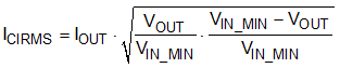
The value of a ceramic capacitor varies significantly over temperature and the amount of DC bias applied to the capacitor. The capacitance variations due to temperature can be minimized by selecting a dielectric material that is stable over temperature. X5R and X7R ceramic dielectrics are usually selected for power regulator capacitors because they have a high capacitance-to-volume ratio and are fairly stable over temperature. The output capacitor must also be selected with the DC bias taken into account. The capacitance value of a capacitor decreases as the DC bias across a capacitor increases. For this example design, a ceramic capacitor with at least a 25-V voltage rating is required to support the maximum input voltage. For this design, one Murata GRM21BR61E226ME44L (10-μF, 25-V, 0805, X5R) capacitor has been selected. The effective capacitance under input voltage of 12 V is 0.18 × 22 = 4 μF. The input capacitance value determines the input ripple voltage of the regulator. The input voltage ripple can be calculated using Equation 19. Using the design example values, IOUT_MAX = 3 A, CIN_E = 4 μF, fSW = 600 kHz, yields an input voltage ripple of 313 mV and a RMS input ripple current of 1.23 A.
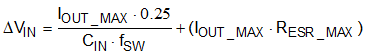
where
- RESR_MAX = the maximum series resistance of the input capacitor