SLUSEH9 October 2021 TPS563212
PRODUCTION DATA
- 1 Features
- 2 Applications
- 3 Description
- 4 Revision History
- 5 Pin Configuration and Functions
- 6 Specifications
-
7 Detailed Description
- 7.1 Overview
- 7.2 Functional Block Diagram
- 7.3
Feature Description
- 7.3.1 Advanced Emulated Current Mode Control
- 7.3.2 Mode Selection and PG/SS Pin Function Configuration
- 7.3.3 Power Good (PG)
- 7.3.4 Soft Start and Pre-Biased Soft Start
- 7.3.5 Output Discharge Through PG/SS Pin
- 7.3.6 Precise Enable and Adjusting Undervoltage Lockout
- 7.3.7 Overcurrent Limit and Undervoltage Protection
- 7.3.8 Overvoltage Protection
- 7.3.9 Thermal Shutdown
- 7.4 Device Functional Modes
- 8 Application and Implementation
- 9 Power Supply Recommendations
- 10Layout
- 11Device and Documentation Support
- 12Mechanical, Packaging, and Orderable Information
Package Options
Mechanical Data (Package|Pins)
- DRL|8
Thermal pad, mechanical data (Package|Pins)
Orderable Information
8.2.2.4 Output Capacitor Selection
After selecting the inductor, the output capacitor needs to be optimized. The LC filter used as the output filter has double pole at:
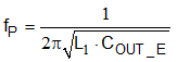
At low frequencies, the overall loop gain is set by the output set-point resistor divider network and the internal gain of the device. The low frequency phase is 180°. At the output filter pole frequency, the gain rolls off at a –40 dB per decade rate and the phase drops rapidly. A high frequency zero introduced by internal circuit that reduces the gain roll off to –20 dB per decade and increases the phase to 90° one decade above the zero frequency. The inductor and capacitor for the output filter must be selected so that the double pole of fP is located below the high frequency zero but close enough. The phase boost provided by the high frequency zero provides adequate phase margin for a stable circuit. To meet this requirement, make the L1 × COUT_E value meet the range of L1 × COUT_E value recommended in Table 8-2.
| OUTPUT VOLTAGE (V)(1) | R8(2) (kΩ) |
R9 (kΩ) |
L1(3) (µH) |
COUT(4) (µF) |
RANGE OF L1 ×
COUT_E(5) (μH × μF) |
C7(6) (pF) |
|---|---|---|---|---|---|---|
| 0.76 | 5.36 | 20.0 | 0.56 | 2×22 | 17–130 | — |
| 1.05 | 15.0 | 20.0 | 0.68 | 2×22 | 17–130 | 10–100 |
| 1.8 | 40.0 | 20.0 | 1.0 | 1×22 | 15–160 | 10–100 |
| 2.5 | 31.6 | 10.0 | 1.5 | 1×22 | 15–160 | 10–100 |
| 3.3 | 45.3 | 10.0 | 2.2 | 1×22 | 15–160 | 10–100 |
| 5 | 73.2 | 10.0 | 3.3 | 1×22 | 15–160 | 10–100 |
The capacitor value and ESR determine the amount of output voltage ripple. The device is intended for use with ceramic or other low-ESR capacitors. Use Equation 17 to determine the required RMS current rating for the output capacitor.
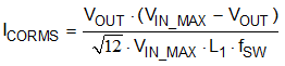
Two Murata GRM21BR61C226ME44L 22-μF, 0805, 16-V output capacitors are used for this design. From the data sheet, the estimated DC derating rate is 66.8% at room temperature with an AC voltage of 0.2 V. The total output effective capacitance is approximately 14.7 μF. The value of L1 × COUT_E is 33 μH × μF, which is within the recommended range.