SLUSEH9 October 2021 TPS563212
PRODUCTION DATA
- 1 Features
- 2 Applications
- 3 Description
- 4 Revision History
- 5 Pin Configuration and Functions
- 6 Specifications
-
7 Detailed Description
- 7.1 Overview
- 7.2 Functional Block Diagram
- 7.3
Feature Description
- 7.3.1 Advanced Emulated Current Mode Control
- 7.3.2 Mode Selection and PG/SS Pin Function Configuration
- 7.3.3 Power Good (PG)
- 7.3.4 Soft Start and Pre-Biased Soft Start
- 7.3.5 Output Discharge Through PG/SS Pin
- 7.3.6 Precise Enable and Adjusting Undervoltage Lockout
- 7.3.7 Overcurrent Limit and Undervoltage Protection
- 7.3.8 Overvoltage Protection
- 7.3.9 Thermal Shutdown
- 7.4 Device Functional Modes
- 8 Application and Implementation
- 9 Power Supply Recommendations
- 10Layout
- 11Device and Documentation Support
- 12Mechanical, Packaging, and Orderable Information
Package Options
Mechanical Data (Package|Pins)
- DRL|8
Thermal pad, mechanical data (Package|Pins)
Orderable Information
7.4.6 On-Time Extension for Large Duty Cycle Operation
The minimum on time, TON_MIN, is the smallest duration of time that the high-side MOSFET can be on. TON_MIN is typically 45 ns in the device. The minimum off time, TOFF_MIN, is the smallest duration that the high-side MOSFET can be off. TOFF_MIN is typically 105 ns in the device. In CCM operation, TON_MIN and TOFF_MIN limit the voltage conversion range given a fixed switching frequency.
The minimum duty cycle allowed is:

The maximum duty cycle allowed is:

In the device, a frequency foldback scheme is employed to extend the maximum duty cycle when TOFF_MIN is reached. The switching frequency decreases once longer duty cycle is needed under low VIN conditions. With the duty increased, the on time is extended up to the maximum on time of 6 μs. A wide range of frequency foldback allows the device output voltage to stay in regulation with a much lower supply voltage VIN. This leads to a lower effective dropout voltage.
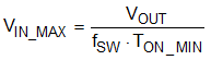
Given an output voltage, the maximum operation supply voltage can be found by:
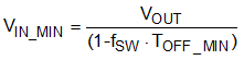
At lower supply voltage, the switching frequency decreases once TOFF_MIN is triggered. The minimum VIN without frequency foldback can be approximated by:
Taking considerations of power losses in the system with heavy load operation, VIN_MAX is higher than the result calculated in Equation 9. With frequency foldback, VIN_VIN is lowered by decreased fSW, as shown in Figure 7-4.