SLUSEN2 April 2022 TPS564242 , TPS564247
PRODUCTION DATA
- 1 Features
- 2 Applications
- 3 Description
- 4 Revision History
- 5 Pin Configuration and Functions
- 6 Specifications
- 7 Detailed Description
- 8 Application and Implementation
- 9 Power Supply Recommendations
- 10Layout
- 11Device and Documentation Support
- 12Mechanical, Packaging, and Orderable Information
Package Options
Mechanical Data (Package|Pins)
- DRL|6
Thermal pad, mechanical data (Package|Pins)
Orderable Information
8.2.2.3 Output Filter Selection
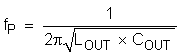
The LC filter used as the output filter has a double pole at Equation 4. In this equation, COUT should use its effective value after derating, not its nominal value.
For any control topology that is compensated internally, there is a range of the output filter it can support. At low frequency, the overall loop gain is set by the output set-point resistor divider network and the internal gain of the device. The low frequency phase is 180°. At the output filter pole frequency, the gain rolls off at a –40 dB per decade rate and the phase drops has a 180 degree drop. The internal ripple generation network introduces a high-frequency zero that reduces the gain roll off from –40 dB to –20 dB per decade and leads the 90 degree phase boost. The internal ripple injection high-frequency zero is about 100 kHz. The inductor and capacitor selected for the output filter is recommended that the double pole is located about 30 kHz, so that the phase boost provided by this high-frequency zero provides adequate phase margin for the stability requirement. The crossover frequency of the overall system should usually be targeted to be less than one-third of the switching frequency (FSW).
| Output Voltage (V) | R1 (kΩ) | R2 (kΩ) | Minimum L1 (μH) | Typical L1 (μH)(1) | Maximum L1 (μH) | Minimum COUT (μF) | Typical COUT (μF)(1) | Maximum COUT (μF) | CFF (pF) |
|---|---|---|---|---|---|---|---|---|---|
| 0.6 | 0 | 10.0 | 0.33 | 0.82 | 2.2 | 22 | 44 | 100 | — |
| 1.05 | 7.5 | 10.0 | 0.47 | 0.82 | 2.2 | 22 | 44 | 100 | — |
| 1.8 | 20.0 | 10.0 | 0.68 | 1.0 | 2.2 | 22 | 44 | 100 | 10–470 |
| 2.5 | 95.0 | 30.0 | 1 | 1.5 | 4.7 | 22 | 44 | 100 | 10–470 |
| 3.3 | 135.0 | 30.0 | 1.2 | 1.5 | 4.7 | 22 | 44 | 100 | 10–470 |
| 5 | 220.0 | 30.0 | 1.5 | 1.8 | 4.7 | 22 | 44 | 100 | 10–470 |
| 7 | 320.0 | 30.0 | 1.8 | 2.2 | 4.7 | 22 | 44 | 100 | 10–470 |
The inductor peak-to-peak ripple current, peak current, and RMS current are calculated using Equation 5, Equation 6, and Equation 7. The inductor saturation current rating must be greater than the calculated peak current and the RMS or heating current rating must be greater than the calculated RMS current.
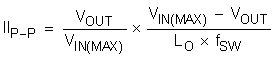
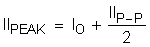
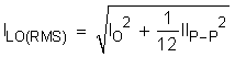
For this design example, the calculated peak current is 4.8 A and the calculated RMS current is 4.2 A. The inductor used is WE744311100 with 8-A saturation current and 15-A rated current.
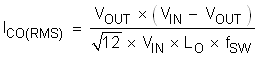
The capacitor value and ESR determines the amount of output voltage ripple. The TPS56424x are intended for use with ceramic or other low-ESR capacitors. Use Equation 8 to determine the required RMS current rating for the output capacitor.
For this design, four MuRata GRM21BR61A226ME44L 22-µF output capacitors are used. The typical ESR is 2 mΩ each. The calculated RMS current is 0.47 A and each output capacitor is rated for 4 A.