SLUSDQ7B May   2020  – December 2023 TPS566231 , TPS566238

PRODUCTION DATA  

  1.   1
  2. Features
  3. Applications
  4. Description
  5. Pin Configuration and Functions
  6. Specifications
    1. 5.1 Absolute Maximum Ratings
    2. 5.2 ESD Ratings
    3. 5.3 Recommended Operating Conditions
    4. 5.4 Thermal Information
    5. 5.5 Electrical Characteristics
    6. 5.6 Typical Characteristics
  7. Detailed Description
    1. 6.1 Overview
    2. 6.2 Functional Block Diagram
    3. 6.3 Feature Description
      1. 6.3.1 PWM Operation and D-CAP3™ Control Mode
      2. 6.3.2 Soft Start
      3. 6.3.3 Power Good
      4. 6.3.4 Large Duty Operation
      5. 6.3.5 Overcurrent Protection and Undervoltage Protection
      6. 6.3.6 Overvoltage Protection
      7. 6.3.7 UVLO Protection
      8. 6.3.8 Output Voltage Discharge
      9. 6.3.9 Thermal Shutdown
    4. 6.4 Device Functional Modes
      1. 6.4.1 Advanced Eco-mode Control
      2. 6.4.2 Force CCM Mode
      3. 6.4.3 Standby Operation
  8. Application and Implementation
    1. 7.1 Application Information
    2. 7.2 Typical Application
      1. 7.2.1 Design Requirements
      2. 7.2.2 Detailed Design Procedure
        1. 7.2.2.1 Custom Design with WEBENCH® Tools
        2. 7.2.2.2 Output Voltage Setpoint
        3. 7.2.2.3 Inductor Selection
        4. 7.2.2.4 Output Capacitor Selection
        5. 7.2.2.5 Input Capacitor Selection
      3. 7.2.3 Application Curves
    3. 7.3 Power Supply Recommendations
    4. 7.4 Layout
      1. 7.4.1 Layout Guidelines
      2. 7.4.2 Layout Example
  9. Device and Documentation Support
    1. 8.1 Device Support
      1. 8.1.1 Development Support
        1. 8.1.1.1 Custom Design with WEBENCH® Tools
    2. 8.2 Receiving Notification of Documentation Updates
    3. 8.3 Support Resources
    4. 8.4 Trademarks
    5. 8.5 Electrostatic Discharge Caution
    6. 8.6 Glossary
  10. Revision History
  11. 10Mechanical, Packaging, and Orderable Information

Package Options

Mechanical Data (Package|Pins)
Thermal pad, mechanical data (Package|Pins)
Orderable Information

Inductor Selection

The inductor ripple current is filtered by the output capacitor. A higher inductor ripple current means the output capacitor must have a ripple current rating higher than the inductor ripple current. See Table 7-2 for recommended inductor values.

The RMS and peak currents through the inductor can be calculated using Equation 5 and Equation 6. Make sure that the inductor is rated to handle these currents.

Equation 5. GUID-9B6CB820-156B-4F6F-9303-9C1B909631DE-low.gif
Equation 6. GUID-2871EBC4-3AEF-45D9-BB54-C6240FB115D0-low.gif

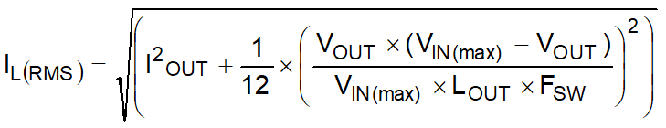
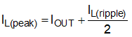
During transient and short-circuit conditions, the inductor current can increase up to the current limit of the device. This means that choosing an inductor with a saturation current higher than the peak current under current limit condition is safe.