SLVSD05H March 2016 – June 2025 TPS56C215
PRODUCTION DATA
- 1
- 1 Features
- 2 Applications
- 3 Description
- 4 Pin Configuration and Functions
- 5 Specifications
-
6 Detailed Description
- 6.1 Overview
- 6.2 Functional Block Diagram
- 6.3
Feature Description
- 6.3.1 PWM Operation and D-CAP3™ Control Mode
- 6.3.2 Eco-mode Control
- 6.3.3 4.7-V LDO
- 6.3.4 MODE Selection
- 6.3.5 Soft Start and Prebiased Soft Start
- 6.3.6 Enable and Adjustable UVLO
- 6.3.7 Power Good
- 6.3.8 Overcurrent Protection and Undervoltage Protection
- 6.3.9 Transient Response Enhancement
- 6.3.10 UVLO Protection
- 6.3.11 Thermal Shutdown
- 6.3.12 Output Voltage Discharge
- 6.4 Device Functional Modes
- 7 Application and Implementation
- 8 Device and Documentation Support
- 9 Revision History
- 10Mechanical, Packaging, and Orderable Information
Package Options
Mechanical Data (Package|Pins)
- RNN|18
Thermal pad, mechanical data (Package|Pins)
Orderable Information
6.3.9 Transient Response Enhancement
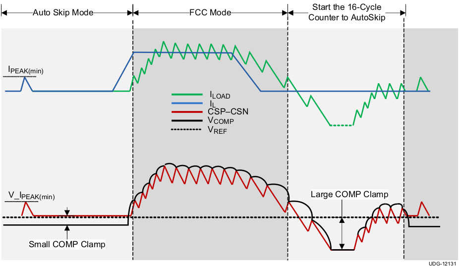
The PSM deglitch feature activates whenever the device transitions from a heavy load in Continuous Conduction Mode (CCM) to a light load in Discontinuous Conduction Mode (DCM). During this transition, the system enters Forced Continuous Conduction Mode (FCCM) for 16 cycles before switching to DCM. This feature is designed to provide fast recovery in load transients during DCM operation.
Figure 6-4 shows 16-cycle and 32-cycle FCCM operation during load release and dynamic COMP pin positioning. Figure 6-5 shows steady-state Auto-skip mode operation with the dynamic COMP pin clamp.
 Figure 6-4 FCCM Transient Response
 Figure 6-5 Auto-skip Mode Transient Response