SLVS324C July 2001 – October 2020 TPS60400 , TPS60401 , TPS60402 , TPS60403
PRODUCTION DATA
- 1 Features
- 2 Applications
- 3 Description
- 4 Revision History
- 5 Device Comparison Table
- 6 Pin Configuration and Functions
- 7 Specifications
- 8 Detailed Description
- 9 Application and Implementation
- 10Power Supply Recommendations
- 11Layout
- 12Device and Documentation Support
- 13Mechanical, Packaging, and Orderable Information
Package Options
Refer to the PDF data sheet for device specific package drawings
Mechanical Data (Package|Pins)
- DBV|5
Thermal pad, mechanical data (Package|Pins)
Orderable Information
3 Description
The TPS6040x family of devices generates an unregulated negative output voltage from an input voltage ranging from 1.6 V to 5.5 V. The devices are typically supplied by a preregulated supply rail of 5 V or 3.3 V. Due to its wide input voltage range, two or three NiCd, NiMH, or alkaline battery cells, as well as one Li-Ion cell can also power them.
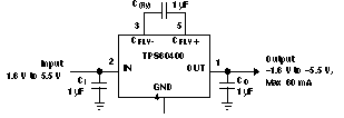
Only three external 1-µF capacitors are required to build a complete DC-DC charge pump inverter. Assembled in a 5-pin SOT-23 package, the complete converter can be built on a 50-mm2 board area. Additional board area and component count reduction is achieved by replacing the Schottky diode that is typically needed for start-up into load by integrated circuitry.
The TPS6040x can deliver a maximum output current of 60 mA with a typical conversion efficiency of greater than 90% over a wide output current range. Three device options with 20-kHz, 50-kHz, and 250-kHz fixed-frequency operation are available. TPS60400 comes with a variable switching frequency to reduce operating current in applications with a wide load range and enables the design with low-value capacitors.
| PART NUMBER | PACKAGE(1) | BODY SIZE (NOM) |
|---|---|---|
| TPS6040x | SOT-23 (5) | 2.90 mm x 1.60 mm |
 Typical Application
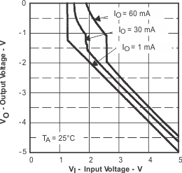
 Output Voltage vs Input
Voltage