SLVS324C July 2001 – October 2020 TPS60400 , TPS60401 , TPS60402 , TPS60403
PRODUCTION DATA
- 1 Features
- 2 Applications
- 3 Description
- 4 Revision History
- 5 Device Comparison Table
- 6 Pin Configuration and Functions
- 7 Specifications
- 8 Detailed Description
- 9 Application and Implementation
- 10Power Supply Recommendations
- 11Layout
- 12Device and Documentation Support
- 13Mechanical, Packaging, and Orderable Information
Package Options
Refer to the PDF data sheet for device specific package drawings
Mechanical Data (Package|Pins)
- DBV|5
Thermal pad, mechanical data (Package|Pins)
Orderable Information
9.2.1.2.4 Output Capacitor (CO)
Increasing the output capacitor's size reduces the output ripple voltage. Decreasing its ESR reduces both output resistance and ripple. Smaller capacitance values can be used with light loads if higher output ripple can be tolerated. Use the following equation to calculate the peak-to-peak ripple.
Equation 6. 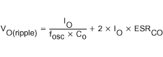
Table 9-1 Recommended Capacitor Values
| DEVICE | VI [V] | IO [mA] | CI [µF] | C(fly) [µF] | CO [µF] |
|---|---|---|---|---|---|
| TPS60400 | 1.8…5.5 | 60 | 1 | 1 | 1 |
| TPS60401 | 1.8…5.5 | 60 | 10 | 10 | 10 |
| TPS60402 | 1.8…5.5 | 60 | 3.3 | 3.3 | 3.3 |
| TPS60403 | 1.8…5.5 | 60 | 1 | 1 | 1 |
Table 9-2 Recommended Capacitors
| MANUFACTURER | PART NUMBER | SIZE | CAPACITANCE | TYPE |
|---|---|---|---|---|
| Taiyo Yuden | EMK212BJ474MG | 0805 | 0.47 µF | Ceramic |
| LMK212BJ105KG | 0805 | 1 µF | Ceramic | |
| LMK212BJ225MG | 0805 | 2.2 µF | Ceramic | |
| EMK316BJ225KL | 1206 | 2.2 µF | Ceramic | |
| LMK316BJ475KL | 1206 | 4.7 µF | Ceramic | |
| JMK316BJ106KL | 1206 | 10 µF | Ceramic | |
| TDK | C2012X5R1C105M | 0805 | 1 µF | Ceramic |
| C2012X5R1A225M | 0805 | 2.2 µF | Ceramic | |
| C2012X5R1A335M | 0805 | 3.3 µF | Ceramic |
Table 9-3 contains a list of manufacturers of the recommended capacitors. Ceramic capacitors will provide the lowest output voltage ripple because they typically have the lowest ESR-rating.
Table 9-3 Recommended Capacitor Manufacturers
| CAPACITOR TYPE | MANUFACTURER | WEB ADDRESS |
|---|---|---|
| X5R / X7R ceramic | Taiyo Yuden | www.t-yuden.com |
| X5R / X7R ceramic | TDK | www.component.tdk.com |
| X5R / X7R ceramic | Vishay | www.vishay.com |
| X5R / X7R ceramic | Kemet | www.kemet.com |