SLVS324C July 2001 – October 2020 TPS60400 , TPS60401 , TPS60402 , TPS60403
PRODUCTION DATA
- 1 Features
- 2 Applications
- 3 Description
- 4 Revision History
- 5 Device Comparison Table
- 6 Pin Configuration and Functions
- 7 Specifications
- 8 Detailed Description
- 9 Application and Implementation
- 10Power Supply Recommendations
- 11Layout
- 12Device and Documentation Support
- 13Mechanical, Packaging, and Orderable Information
Package Options
Refer to the PDF data sheet for device specific package drawings
Mechanical Data (Package|Pins)
- DBV|5
Thermal pad, mechanical data (Package|Pins)
Orderable Information
7.6 Typical Characteristics
Table 7-1 Table of Graphs
| FIGURE | |||
|---|---|---|---|
| η | Efficiency | vs Output current at 3.3 V, 5 V TPS60400, TPS60401, TPS60402, TPS60403 | Figure 7-1, Figure 7-2 |
| II | Input current | vs Output current TPS60400, TPS60401, TPS60402, TPS60403 | Figure 7-3, Figure 7-4 |
| IS | Supply current | vs Input voltage TPS60400, TPS60401, TPS60402, TPS60403 | Figure 7-5, Figure 7-6 |
| Output resistance | vs Input voltage at -40°C, 0°C, 25°C, 85°C TPS60400, CI = C(fly) = CO = 1 µF TPS60401, CI = C(fly) = CO = 10 µF TPS60402 , CI = C(fly) = CO = 3.3 µF TPS60403, CI = C(fly) = CO = 1 µF | Figure 7-7, Figure 7-8, Figure 7-9, Figure 7-10 | |
| VO | Output voltage | vs Output current at 25°C, VIN=1.8 V, 2.5 V, 3.3 V, 5 V TPS60400, CI = C(fly) = CO = 1 µF TPS60401, CI = C(fly) = CO = 10 µF TPS60402 , CI = C(fly) = CO = 3.3 µF TPS60403, CI = C(fly) = CO = 1 µF | Figure 7-11, Figure 7-12, Figure 7-13, Figure 7-14 |
| fOSC | Oscillator frequency | vs Temperature at VI = 1.8 V, 2.5 V, 3.3 V, 5 V TPS60400, TPS60401, TPS60402, TPS60403 | Figure 7-15, Figure 7-16, Figure 7-17, Figure 7-18 |
| fOSC | Oscillator frequency | vs Output current TPS60400 at 2 V, 3.3 V, 5.0 V | Figure 7-19 |
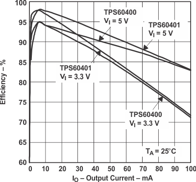 Figure 7-1 Efficiency vs Output Current
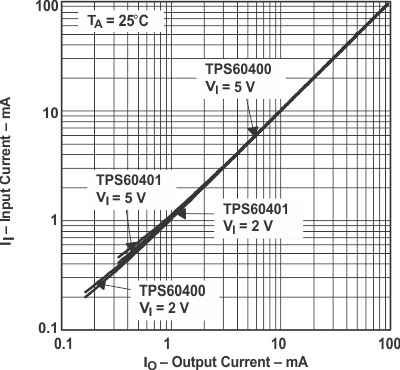 Figure 7-3 Input Current vs Output Current
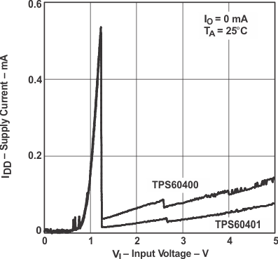 Figure 7-5 Supply Current vs Input Voltage
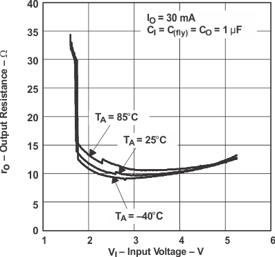 Figure 7-7 Output Resistance vs Input Voltage
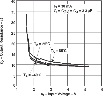 Figure 7-9 Output Resistance vs Input Voltage
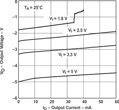 Figure 7-11 Output Voltage vs Output Current
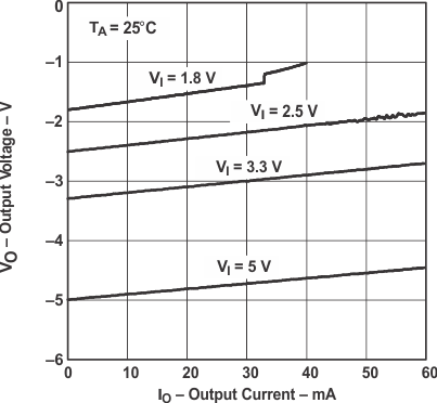 Figure 7-13 Output Voltage vs Output Current
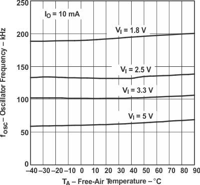 Figure 7-15 Oscillator Frequency vs Free-Air Temperature
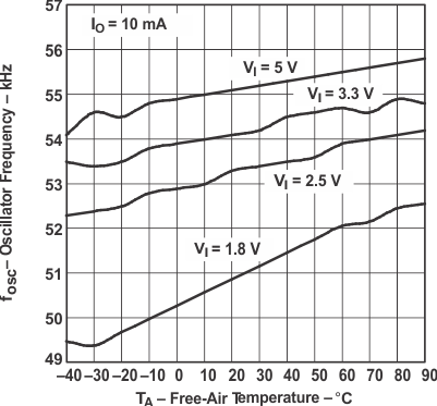 Figure 7-17 Oscillator Frequency vs Free-Air Temperature
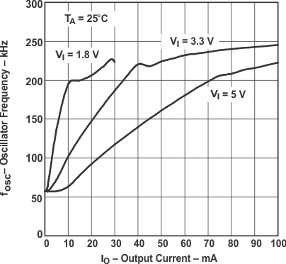 Figure 7-19 Oscillator Frequency vs Output Current
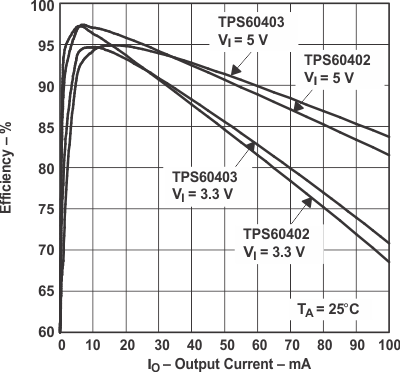 Figure 7-2 Efficiency vs Output Current
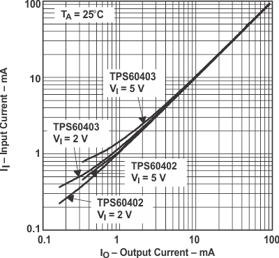 Figure 7-4 Input Current vs Output Current
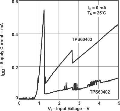 Figure 7-6 Supply Current vs Input Voltage
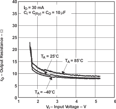 Figure 7-8 Output Resistance vs Input Voltage
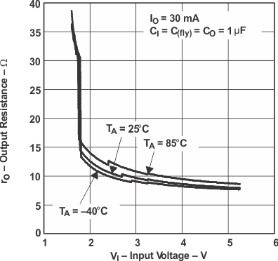 Figure 7-10 Output Resistance vs Input Voltage
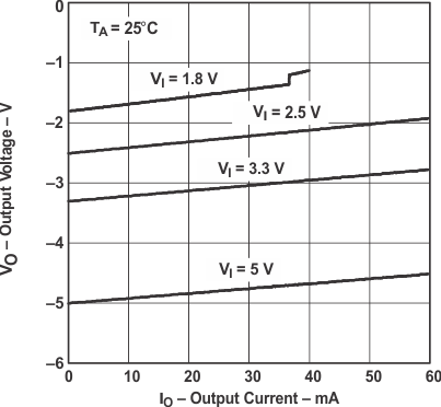 Figure 7-12 Output Voltage vs Output Current
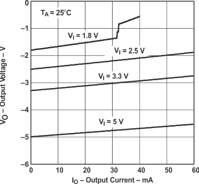 Figure 7-14 Output Voltage vs Output Current
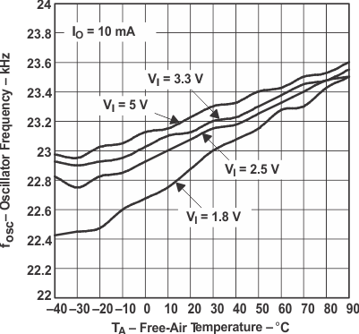 Figure 7-16 Oscillator Frequency vs Free-Air Temperature
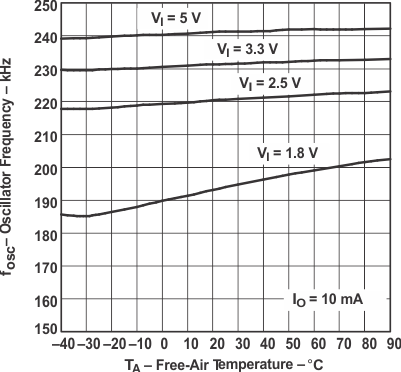 Figure 7-18 Oscillator Frequency vs Free-Air Temperature