SLVS324C July 2001 – October 2020 TPS60400 , TPS60401 , TPS60402 , TPS60403
PRODUCTION DATA
- 1 Features
- 2 Applications
- 3 Description
- 4 Revision History
- 5 Device Comparison Table
- 6 Pin Configuration and Functions
- 7 Specifications
- 8 Detailed Description
- 9 Application and Implementation
- 10Power Supply Recommendations
- 11Layout
- 12Device and Documentation Support
- 13Mechanical, Packaging, and Orderable Information
Package Options
Refer to the PDF data sheet for device specific package drawings
Mechanical Data (Package|Pins)
- DBV|5
Thermal pad, mechanical data (Package|Pins)
Orderable Information
8.3.2 Efficiency Considerations
The power efficiency of a switched-capacitor voltage converter is affected by three factors: the internal losses in the converter IC, the resistive losses of the capacitors, and the conversion losses during charge transfer between the capacitors. The internal losses are associated with the internal functions of the IC, such as driving the switches, oscillator, and so forth. These losses are affected by operating conditions such as input voltage, temperature, and frequency. The next two losses are associated with the output resistance of the voltage converter circuit. Switch losses occur because of the on-resistance of the MOSFET switches in the IC. Charge-pump capacitor losses occur because of their ESR. The relationship between these losses and the output resistance is as follows:
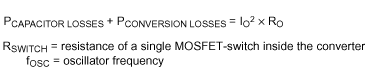
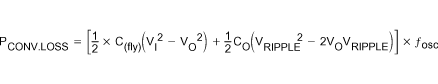
The first term is the effective resistance from an ideal switched-capacitor circuit. Conversion losses occur during the charge transfer between C(fly) and CO when there is a voltage difference between them. The power loss is:
The efficiency of the TPS6040x devices is dominated by their quiescent supply current at low output current and by their output impedance at higher current.
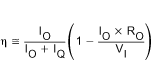
Where, IQ = quiescent current.