SLVSDX7D January 2019 – July 2021 TPS61022
PRODUCTION DATA
- 1 Features
- 2 Applications
- 3 Description
- 4 Revision History
- 5 Pin Configuration and Functions
- 6 Specifications
- 7 Detailed Description
- 8 Application and Implementation
- 9 Power Supply Recommendations
- 10Layout
- 11Device and Documentation Support
- 12Mechanical, Packaging, and Orderable Information
Package Options
Mechanical Data (Package|Pins)
- RWU|7
Thermal pad, mechanical data (Package|Pins)
Orderable Information
8.2.2.4 Loop Stability, Feedforward Capacitor Selection
When the switching waveform shows large duty cycle jitter or the output voltage or inductor current shows oscillations, the regulation loop may be unstable.
The load transient response is another approach to check the loop stability. During the load transient recovery time, VOUT can be monitored for settling time, overshoot or ringing that helps judge the stability of the converters. Without any ringing, the loop has usually more than 45° of phase margin.
A feedforward capacitor (C3 in the Figure 8-2) in parallel with R1 induces a pair of zero and pole in the loop transfer function. By setting the proper zero frequency, the feedforward capacitor can increase the phase margin to improve the loop stability. For large output capacitance more than 40 μF application, TI recommends a feedforward capacitor to set the zero frequency (fFFZ) to 2 kHz. As for the input voltage lower than 2-V application, TI recommends setting the zero frequency (fFFZ) to 20 kHz when the effective output capacitance is less than 40 μF. The value of the feedforward capacitor can be calculated by Equation 10.
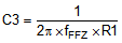
where
- R1 is the resistor between the VOUT pin and FB pin
- fFFZ is the zero frequency created by the feedforward capacitor
 Figure 8-2 TPS61022 Circuit With Feedforward Capacitor