SLVS413K October 2002 – July 2022 TPS61040 , TPS61041
PRODUCTION DATA
- 1 Features
- 2 Applications
- 3 Description
- 4 Revision History
- 5 Pin Configuration and Functions
- 6 Specifications
- 7 Detailed Description
- 8 Application and Implementation
- 9 Power Supply Recommendations
- 10Layout
- 11Device and Documentation Support
- 12Mechanical, Packaging, and Orderable Information
Package Options
Refer to the PDF data sheet for device specific package drawings
Mechanical Data (Package|Pins)
- DBV|5
- DRV|6
Thermal pad, mechanical data (Package|Pins)
- DRV|6
Orderable Information
8.3 System Examples
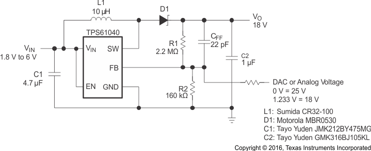 Figure 8-5 LCD Bias Supply With Adjustable Output Voltage
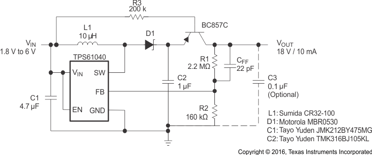 Figure 8-6 LCD Bias Supply With Load Disconnect
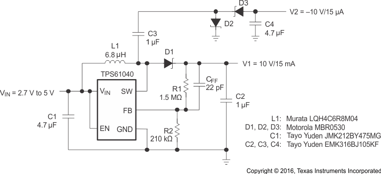 Figure 8-7 Positive
and Negative Output LCD Bias Supply
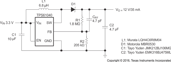 Figure 8-8 Standard 3.3-V to 12-V Supply
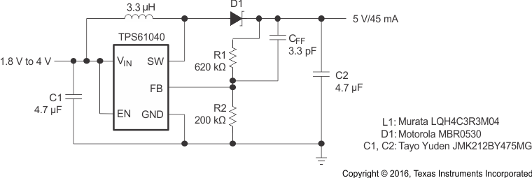 Figure 8-9 Dual Battery Cell to 5-V/50-mA Conversion Efficiency Approximately Equals 84% at VIN = 2.4 V to Vo = 5 V/45 mA
 Figure 8-10 White LED Supply With Adjustable Brightness Control Using a PWM Signal on the Enable Pin, Efficiency Approximately Equals 86% at VIN = 3 V, ILED = 15 mA
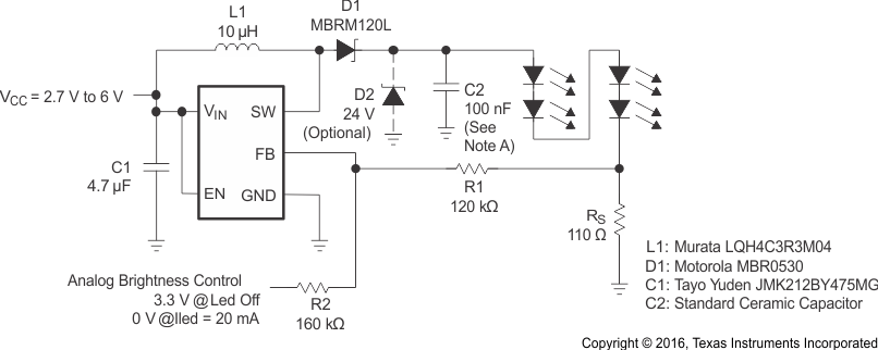
A. A smaller output capacitor value for C2 causes a larger LED ripple.
Figure 8-11 White LED Supply With Adjustable Brightness Control Using an Analog Signal on the Feedback Pin