SLVS413K October 2002 – July 2022 TPS61040 , TPS61041
PRODUCTION DATA
- 1 Features
- 2 Applications
- 3 Description
- 4 Revision History
- 5 Pin Configuration and Functions
- 6 Specifications
- 7 Detailed Description
- 8 Application and Implementation
- 9 Power Supply Recommendations
- 10Layout
- 11Device and Documentation Support
- 12Mechanical, Packaging, and Orderable Information
Package Options
Refer to the PDF data sheet for device specific package drawings
Mechanical Data (Package|Pins)
- DBV|5
- DRV|6
Thermal pad, mechanical data (Package|Pins)
- DRV|6
Orderable Information
8.2.2.4 Output Capacitor Selection
For best output voltage filtering, a low ESR output capacitor is recommended. Ceramic capacitors have a low ESR value but tantalum capacitors can be used as well, depending on the application.
Assuming the converter does not show double pulses or pulse bursts on the switch node (SW), the output voltage ripple can be calculated as:
Equation 7. 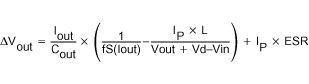
where
- IP = Peak current as described in Peak Current Control
- L = Selected inductor value
- Iout = Nominal load current
- fS (Iout) = Switching frequency at the nominal load current as calculated previously
- Vd = Rectifier diode forward voltage (typically 0.3 V)
- Cout = Selected output capacitor
- ESR = Output capacitor ESR value
See Table 8-3 and the Typical Application for choosing the output capacitor.
Table 8-3 Recommended Input and Output Capacitors
| DEVICE | CAPACITOR | VOLTAGE RATING | COMPONENT SUPPLIER(1) | COMMENTS |
|---|---|---|---|---|
| TPS6104x | 4.7 μF/X5R/0805 | 6.3 V | Tayo Yuden JMK212BY475MG | CIN/COUT |
| 10 μF/X5R/0805 | 6.3 V | Tayo Yuden JMK212BJ106MG | CIN/COUT | |
| 1 μF/X7R/1206 | 25 V | Tayo Yuden TMK316BJ105KL | COUT | |
| 1 μF/X5R/1206 | 35 V | Tayo Yuden GMK316BJ105KL | COUT | |
| 4.7 μF/X5R/1210 | 25 V | Tayo Yuden TMK325BJ475MG | COUT |
(1) See Third-Party Products disclaimer.