SLVSCM8D May 2015 – August 2021 TPS61088
PRODUCTION DATA
- 1 Features
- 2 Applications
- 3 Description
- 4 Revision History
- 5 Pin Configuration and Functions
- 6 Specifications
- 7 Detailed Description
- 8 Application and Implementation
- 9 Power Supply Recommendations
- 10Layout
- 11Device and Documentation Support
- 12Mechanical, Packaging, and Orderable Information
Package Options
Mechanical Data (Package|Pins)
- RHL|20
Thermal pad, mechanical data (Package|Pins)
- RHL|20
Orderable Information
5 Pin Configuration and Functions
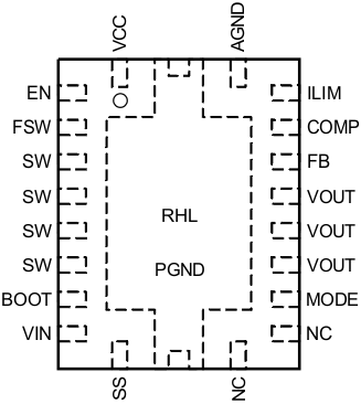
 Figure 5-1 20-Pin VQFN With Thermal Pad
RHL Package(Top View)
Figure 5-1 20-Pin VQFN With Thermal Pad
RHL Package(Top View)Table 5-1 Pin Functions
| PIN | I/O | DESCRIPTION | |
|---|---|---|---|
| NAME | NUMBER | ||
| VCC | 1 | O | Output of the internal regulator. A ceramic capacitor of more than 1.0 µF is required between this pin and ground. |
| EN | 2 | I | Enable logic input. Logic high level enables the device. Logic low level disables the device and turns it into shutdown mode. |
| FSW | 3 | I | The switching frequency is programmed by a resistor between this pin and the SW pin. |
| SW | 4, 5, 6, 7 | I | The switching node pin of the converter. It is connected to the drain of the internal low-side power MOSFET and the source of the internal high-side power MOSFET. |
| BOOT | 8 | O | Power supply for high-side MOSFET gate driver. A ceramic capacitor of 0.1 µF must be connected between this pin and the SW pin. |
| VIN | 9 | I | IC power supply input |
| SS | 10 | O | Soft-start programming pin. An external capacitor sets the ramp rate of the reference voltage of the internal error amplifier during soft start. |
| NC | 11, 12 | — | No connection inside the device. Connect these two pins to the ground plane on the PCB for good thermal dissipation. |
| MODE | 13 | I | Operation mode selection pin for the device in light load condition. When this pin is connected to ground, the device works in PWM mode. When this pin is left floating, the device works in PFM mode. |
| VOUT | 14, 15, 16 | O | Boost converter output |
| FB | 17 | I | Voltage feedback. Connect to the center tape of a resistor divider to program the output voltage. |
| COMP | 18 | O | Output of the internal error amplifier, the loop compensation network must be connected between this pin and the AGND pin. |
| ILIM | 19 | O | Adjustable switch peak current limit. An external resistor must be connected between this pin and the AGND pin. |
| AGND | 20 | — | Signal ground of the IC |
| PGND | 21 | — | Power ground of the IC. It is connected to the source of the low-side MOSFET. |