SLVSD38C November 2015 – August 2021 TPS61089
PRODMIX
- 1 Features
- 2 Applications
- 3 Description
- 4 Revision History
- 5 Device Comparison Table
- 6 Pin Configuration and Functions
- 7 Specifications
- 8 Detailed Description
- 9 Application and Implementation
- 10Power Supply Recommendations
- 11Layout
- 12Device and Documentation Support
- 13Mechanical, Packaging, and Orderable Information
Package Options
Mechanical Data (Package|Pins)
- RNR|11
Thermal pad, mechanical data (Package|Pins)
Orderable Information
9.2.2.2 Setting Switching Frequency
The switching frequency is set by a resistor connected between the FSW pin and the SW pin of the TPS61089x. The resistor value required for a desired frequency can be calculated using Equation 3.
Equation 3.
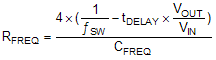
where
- RFREQ is the resistance connected between the FSW pin and the SW pin
- CFREQ = 24 pF
- ƒSW is the desired switching frequency
- tDELAY = 86 ns
- VIN is the input voltage
- VOUT is the output voltage