SLVSFH6C January   2021  – December 2021 TPS61094

PRODUCTION DATA  

  1. Features
  2. Applications
  3. Description
  4. Revision History
  5. Pin Configuration and Functions
  6. Specifications
    1. 6.1 Absolute Maximum Ratings
    2. 6.2 ESD Ratings
    3. 6.3 Recommended Operating Conditions
    4. 6.4 Thermal Information
    5. 6.5 Electrical Characteristics
    6. 6.6 Typical Characteristics
  7. Detailed Description
    1. 7.1 Overview
      1. 7.1.1 The Configuration of VCHG Pin, ICHG Pin, and OSEL Pin
        1. 7.1.1.1 OSEL: Output Voltage Selection
        2. 7.1.1.2 VCHG: Charging Termination Voltage Selection
        3. 7.1.1.3 ICHG: Charging Output Current Selection
    2. 7.2 Functional Block Diagram
    3. 7.3 Feature Description
      1. 7.3.1 Undervoltage Lockout
      2. 7.3.2 Enable and Soft Start
      3. 7.3.3 Active Pulldown for the EN and MODE Pins
      4. 7.3.4 Current Limit Operation
      5. 7.3.5 Output Short-to-Ground Protection
      6. 7.3.6 Thermal Shutdown
    4. 7.4 Device Functional Modes
      1. 7.4.1 Operation Mode Setting
      2. 7.4.2 Forced Bypass Mode Operation
      3. 7.4.3 True Shutdown Mode Operation
      4. 7.4.4 Forced Buck Mode Operation
      5. 7.4.5 Auto Buck or Boost Mode Operation
        1. 7.4.5.1 Three States (Boost_on, Buck_on, and Supplement) Transition
        2. 7.4.5.2 Boost, Bypass, and Pass-Through
        3. 7.4.5.3 PWM, PFM, and Snooze Modes in Boost Operation
          1. 7.4.5.3.1 PWM Mode
          2. 7.4.5.3.2 PFM Mode
          3. 7.4.5.3.3 Snooze Mode
  8. Application and Implementation
    1. 8.1 Application Information
    2. 8.2 Typical Application – 3.6-V Output Boost Converter with Bypass
      1. 8.2.1 Design Requirements
      2. 8.2.2 Detailed Design Procedure
        1. 8.2.2.1 Programming the Output Voltage
        2. 8.2.2.2 Maximum Output Current
        3. 8.2.2.3 Inductor Selection
        4. 8.2.2.4 Output Capacitor Selection
        5. 8.2.2.5 Input Capacitor Selection
      3. 8.2.3 Application Curves
      4. 8.2.4 Typical Application – 3.3-V Output Boost Converter with Automatic Buck or Boost Function
        1. 8.2.4.1 Design Requirements
        2. 8.2.4.2 Detailed Design Procedure
          1. 8.2.4.2.1 Programming the Voltage and Current
        3. 8.2.4.3 Application Curves
  9. Power Supply Recommendations
  10. 10Layout
    1. 10.1 Layout Guidelines
    2. 10.2 Layout Example
  11. 11Device and Documentation Support
    1. 11.1 Device Support
      1. 11.1.1 Third-Party Products Disclaimer
    2. 11.2 Documentation Support
      1. 11.2.1 Related Documentation
    3. 11.3 Receiving Notification of Documentation Updates
    4. 11.4 Support Resources
    5. 11.5 Trademarks
    6. 11.6 Electrostatic Discharge Caution
    7. 11.7 Glossary
  12. 12Mechanical, Packaging, and Orderable Information

Package Options

Mechanical Data (Package|Pins)
Thermal pad, mechanical data (Package|Pins)
Orderable Information

Application Curves

GUID-20201126-CA0I-M4BK-SZNT-RD2PZ7KX9XL6-low.gif
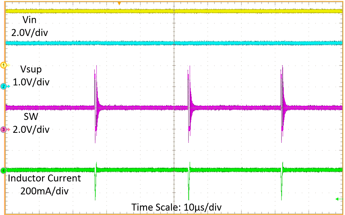
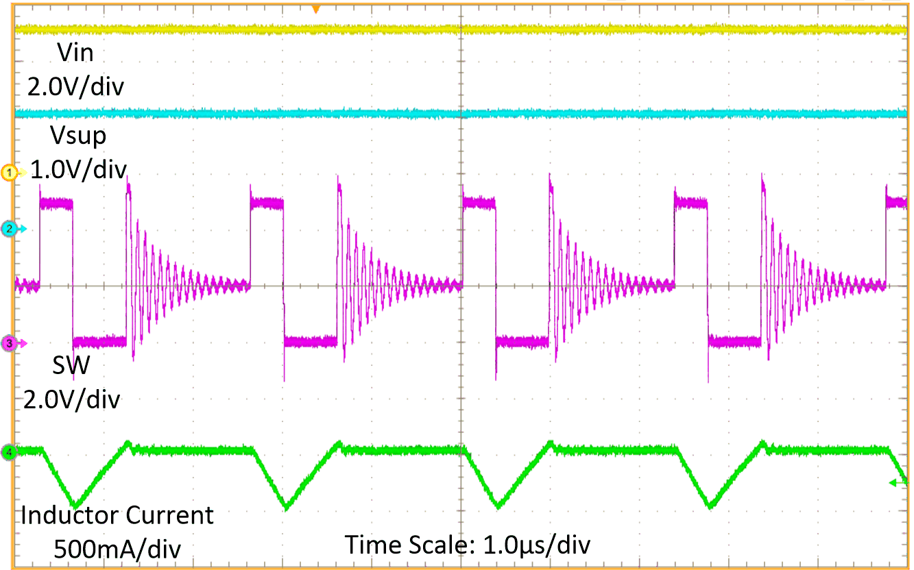
VIN = 5 V VSUP = 2 V
Figure 8-15 Switching Waveform at Buck Mode with ICHG = 2.5 mA
GUID-20201126-CA0I-KHX6-6PJL-SQN5W5RLKV8W-low.gif
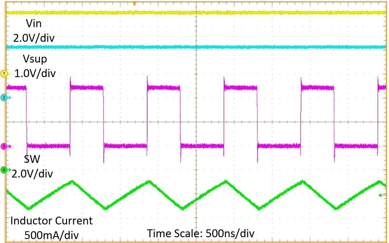
VIN = 5 V VSUP = 2 V
Figure 8-17 Switching Waveform at Buck Mode with ICHG = 500mA
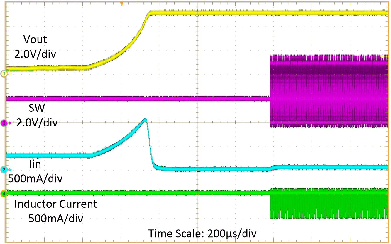
GUID-20201126-CA0I-1S2Z-J8ZB-RQ7LGC0LW984-low.gif
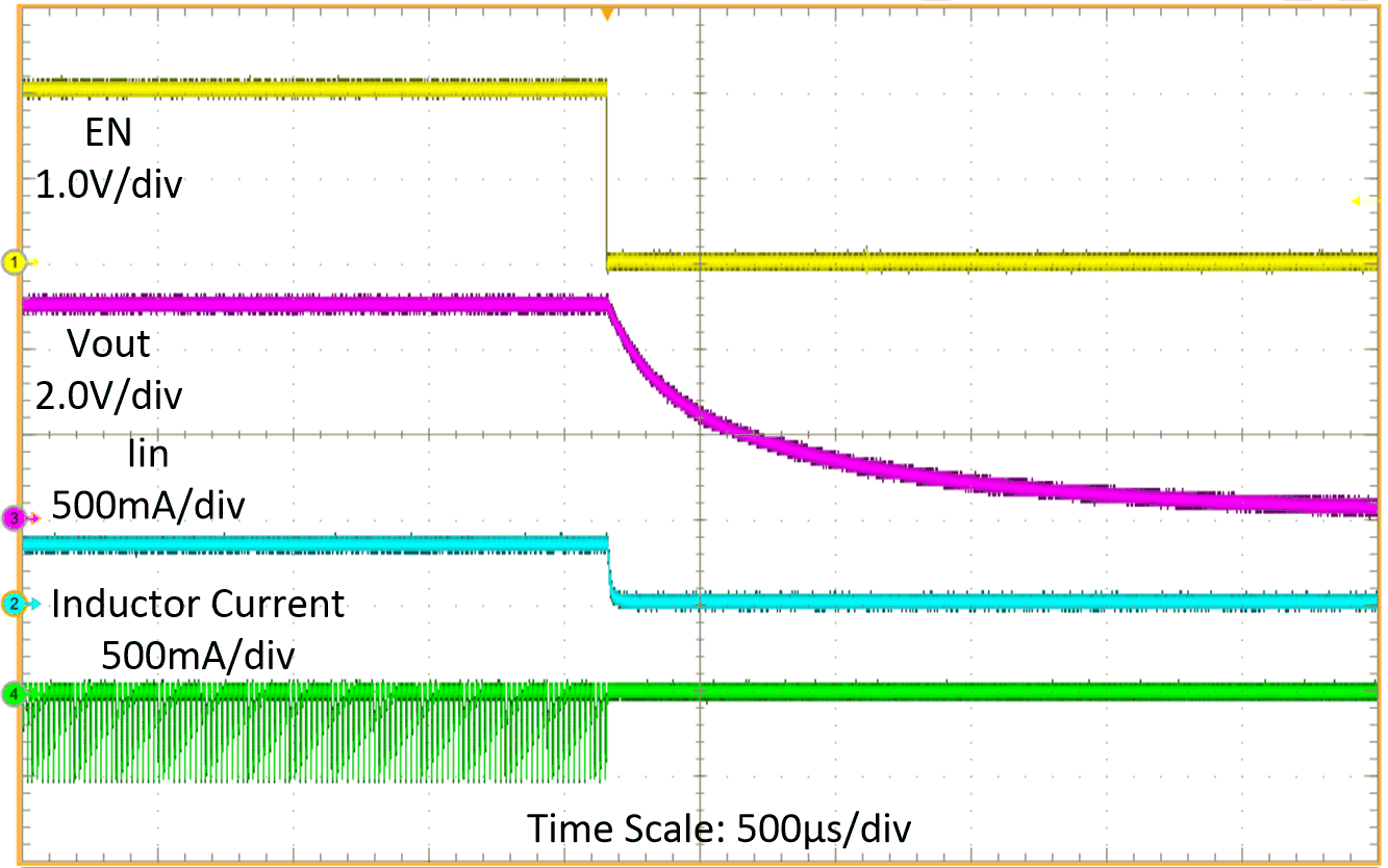
VIN = 5 V VSUP = 0 V Rload = 15 Ω
Figure 8-19 Shutdown by EN
GUID-20201126-CA0I-SBGJ-S8QW-CBVTRPBFGNFV-low.gif
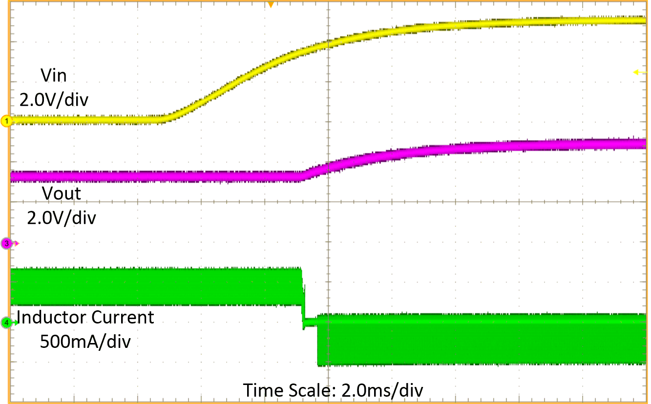
VIN = 5 V VSUP = 2 V Iout = 250 mA
Figure 8-21 VIN Power On and Charging Automatically
GUID-20201126-CA0I-DWHX-M5B3-MRLDJDSHLPP0-low.gif
VIN = 5 V VSUP = 2 V Open load
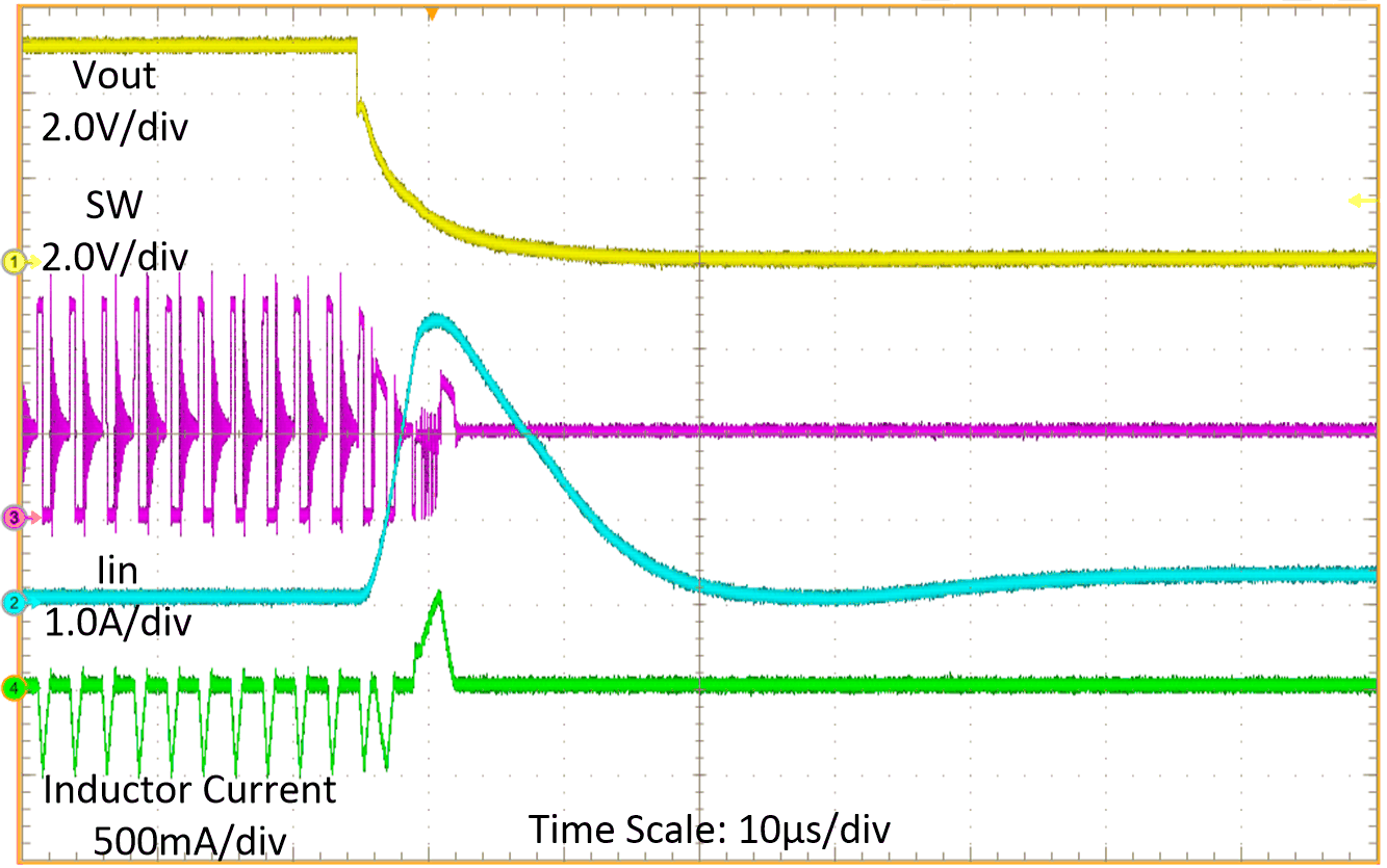
Figure 8-23 Output Short Protection (Recover)
GUID-20201126-CA0I-NRQR-08FS-8MBBCWLZQP9K-low.gif
VIN = 5 V VSUP = 2 V
Figure 8-16 Switching Waveform at Buck Mode with ICHG = 100 mA
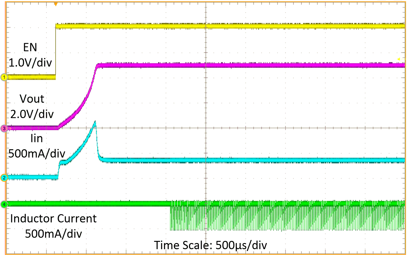
GUID-20201126-CA0I-3V8P-LSNX-N5LH4WDZ8XN8-low.gif
VIN = 5 V VSUP = 0 V Rload = 15 Ω
Figure 8-18 Start-Up by EN
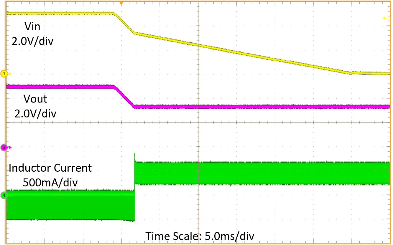
GUID-20201126-CA0I-NR1D-XFFH-BRQC6TS41XP0-low.gif
VIN = 5 V VSUP = 2 V Iout = 250 mA
Figure 8-20 VIN Power Down and Backup Automatically
GUID-20201126-CA0I-TL49-Z5BZ-C0RWH3KPZMM8-low.gif
VIN = 5 V VSUP = 2 V Open load
Figure 8-22 Output Short Protection (Entry)