SLVSFH6C January   2021  – December 2021 TPS61094

PRODUCTION DATA  

  1. Features
  2. Applications
  3. Description
  4. Revision History
  5. Pin Configuration and Functions
  6. Specifications
    1. 6.1 Absolute Maximum Ratings
    2. 6.2 ESD Ratings
    3. 6.3 Recommended Operating Conditions
    4. 6.4 Thermal Information
    5. 6.5 Electrical Characteristics
    6. 6.6 Typical Characteristics
  7. Detailed Description
    1. 7.1 Overview
      1. 7.1.1 The Configuration of VCHG Pin, ICHG Pin, and OSEL Pin
        1. 7.1.1.1 OSEL: Output Voltage Selection
        2. 7.1.1.2 VCHG: Charging Termination Voltage Selection
        3. 7.1.1.3 ICHG: Charging Output Current Selection
    2. 7.2 Functional Block Diagram
    3. 7.3 Feature Description
      1. 7.3.1 Undervoltage Lockout
      2. 7.3.2 Enable and Soft Start
      3. 7.3.3 Active Pulldown for the EN and MODE Pins
      4. 7.3.4 Current Limit Operation
      5. 7.3.5 Output Short-to-Ground Protection
      6. 7.3.6 Thermal Shutdown
    4. 7.4 Device Functional Modes
      1. 7.4.1 Operation Mode Setting
      2. 7.4.2 Forced Bypass Mode Operation
      3. 7.4.3 True Shutdown Mode Operation
      4. 7.4.4 Forced Buck Mode Operation
      5. 7.4.5 Auto Buck or Boost Mode Operation
        1. 7.4.5.1 Three States (Boost_on, Buck_on, and Supplement) Transition
        2. 7.4.5.2 Boost, Bypass, and Pass-Through
        3. 7.4.5.3 PWM, PFM, and Snooze Modes in Boost Operation
          1. 7.4.5.3.1 PWM Mode
          2. 7.4.5.3.2 PFM Mode
          3. 7.4.5.3.3 Snooze Mode
  8. Application and Implementation
    1. 8.1 Application Information
    2. 8.2 Typical Application – 3.6-V Output Boost Converter with Bypass
      1. 8.2.1 Design Requirements
      2. 8.2.2 Detailed Design Procedure
        1. 8.2.2.1 Programming the Output Voltage
        2. 8.2.2.2 Maximum Output Current
        3. 8.2.2.3 Inductor Selection
        4. 8.2.2.4 Output Capacitor Selection
        5. 8.2.2.5 Input Capacitor Selection
      3. 8.2.3 Application Curves
      4. 8.2.4 Typical Application – 3.3-V Output Boost Converter with Automatic Buck or Boost Function
        1. 8.2.4.1 Design Requirements
        2. 8.2.4.2 Detailed Design Procedure
          1. 8.2.4.2.1 Programming the Voltage and Current
        3. 8.2.4.3 Application Curves
  9. Power Supply Recommendations
  10. 10Layout
    1. 10.1 Layout Guidelines
    2. 10.2 Layout Example
  11. 11Device and Documentation Support
    1. 11.1 Device Support
      1. 11.1.1 Third-Party Products Disclaimer
    2. 11.2 Documentation Support
      1. 11.2.1 Related Documentation
    3. 11.3 Receiving Notification of Documentation Updates
    4. 11.4 Support Resources
    5. 11.5 Trademarks
    6. 11.6 Electrostatic Discharge Caution
    7. 11.7 Glossary
  12. 12Mechanical, Packaging, and Orderable Information

Package Options

Mechanical Data (Package|Pins)
Thermal pad, mechanical data (Package|Pins)
Orderable Information

Current Limit Operation

The TPS61094 has the peak current limit in Buck mode and valley current limit in Boost mode. Current limit detection occurs when the high-side MOSFET turns on.

In Buck mode, the TPS61094 has average output current control, so the current limit in Buck mode is hard to reach.

In Boost mode, when the load current is increased such that the inductor current is above the current limit within the whole switching cycle time, the off time is increased to allow the inductor current to decrease to this threshold before the next on time begins (called the frequency foldback mechanism). When the current limit is reached, the output voltage decreases during further load increase.

The maximum continuous output current (IOUT(LC)), before entering current limit (CL) operation, can be defined by Equation 1.
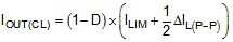
Equation 1. GUID-89660ACD-6268-447B-A24D-F636020BD9B0-low.gif

where

  • D is the duty cycle.
  • ΔIL(P-P) is the inductor ripple current.

The duty cycle can be estimated by Equation 2.

Equation 2. GUID-BDAD3DD2-E490-443F-87D8-CDCBC47F71C9-low.gif

where

  • VOUT is the output voltage of the boost converter.
  • VIN is the input voltage of the boost converter.
  • η is the efficiency of the converter; use 90% for most applications.

The peak-to-peak inductor ripple current is calculated by Equation 3.
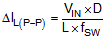
Equation 3. GUID-BF92EE92-5D67-4B97-B729-EA4F0188D0EB-low.gif

where

  • L is the inductance value of the inductor.
  • fSW is the switching frequency.
  • D is the duty cycle.
  • VIN is the input voltage of the boost converter.