SLVS873F June 2015 – September 2021 TPS61098 , TPS610981 , TPS610982 , TPS610985 , TPS610986 , TPS610987
PRODUCTION DATA
- 1 Features
- 2 Applications
- 3 Description
- 4 Revision History
- 5 Device Comparison Table
- 6 Pin Configuration and Functions
- 7 Specifications
- 8 Detailed Description
- 9 Applications and Implementation
- 10Power Supply Recommendations
- 11Layout
- 12Device and Documentation Support
- 13Mechanical, Packaging, and Orderable Information
Package Options
Mechanical Data (Package|Pins)
- DSE|6
Thermal pad, mechanical data (Package|Pins)
Orderable Information
3 Description
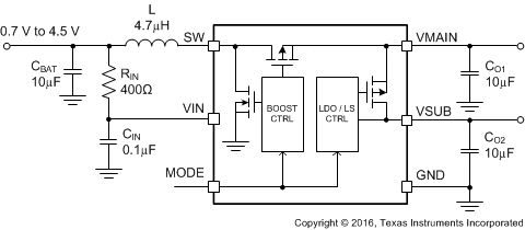
The TPS61098x is an ultra-low power solution for products powered by either a one-cell or two-cell alkaline, NiCd or NiMH, one-cell coin cell or one-cell Li-Ion or Li-polymer battery. It integrates either a Low-dropout Linear Regulator (LDO) or a load switch with a boost converter and provides two output rails. The boost output V(MAIN) is designed as an always-on supply for a main system, and the LDO or load switch output V(SUB) is to power peripheral devices.
The TPS61098x has two modes controlled by the MODE pin: Active mode and Low Power mode. In Active mode, both outputs are enabled with enhanced response performance. In Low Power mode, the LDO or load switch is disabled to disconnect peripherals. The TPS61098x consumes only 300-nA quiescent current and can achieve up to 88% efficiency at 10-µA load in Low Power mode.
The TPS61098x supports automatic pass-through function. When input voltage is higher than a pass-through threshold, the boost converter stops switching and passes the input voltage to the VMAIN rail; when input voltage is lower than the threshold, the boost works in Boost mode and regulates the output at the target value. The TPS61098x provides different versions for different output set values.
The TPS61098x can provide up to 50-mA total output current at 0.7-V input to 3.3-V output conversion. The boost is based on a hysteretic controller topology using a synchronous rectifier to obtain maximum efficiency at minimal quiescent current.
The TPS61098x is available in 1.5-mm × 1.5-mm WSON package to enable small circuit layout size.
| PART NUMBER | PACKAGE(1) | BODY SIZE (NOM) |
|---|---|---|
| TPS61098x | 6 Pin WSON | 1.50 mm × 1.50 mm |
 Simplified Schematic