SLVS873F June 2015 – September 2021 TPS61098 , TPS610981 , TPS610982 , TPS610985 , TPS610986 , TPS610987
PRODUCTION DATA
- 1 Features
- 2 Applications
- 3 Description
- 4 Revision History
- 5 Device Comparison Table
- 6 Pin Configuration and Functions
- 7 Specifications
- 8 Detailed Description
- 9 Applications and Implementation
- 10Power Supply Recommendations
- 11Layout
- 12Device and Documentation Support
- 13Mechanical, Packaging, and Orderable Information
Package Options
Mechanical Data (Package|Pins)
- DSE|6
Thermal pad, mechanical data (Package|Pins)
Orderable Information
8.3.3 LDO / Load Switch Operation
The TPS61098x uses a PMOS as a pass element of its integrated LDO / load switch. The input of the PMOS is connected to the output of the boost converter. When the MODE pin is pulled logic high, the PMOS is enabled to output a voltage on VSUB pin.
For load switch version, the PMOS pass element is fully turned on when enabled, no matter the boost converter works in boost operation mode or pass-through operation mode. So the output voltage at VSUB pin is decided by the output voltage at VMAIN pin and the current passing through the PMOS as Equation 2:
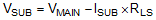
where
- I(SUB) is the load of VSUB rail
- RLS is the resistance of the PMOS when it is fully turned on
For LDO version, the output voltage V(SUB) is regulated at the set value when the voltage difference between its input and output is higher than the dropout voltage V(Dropout), no matter the boost converter works in boost operation mode or pass-through operation mode. The V(SUB) is monitored via an internal feedback network which is connected to the voltage error amplifier. To regulate V(SUB), the voltage error amplifier compares the feedback voltage to the internal voltage reference and adjusts the gate voltage of the PMOS accordingly. When the voltage drop across the PMOS is lower than the dropout voltage, the PMOS will be fully turned on and the output voltage at V(SUB) is decided by Equation 2.
When the MODE pin is pulled low, the LDO or load switch is turned off to disconnect the load at VSUB pin. For some versions, active discharge function at VSUB pin is offered, which can discharge the V(SUB) to ground after MODE pin is pulled low, to avoid any bias condition to downstream devices. For versions without the active discharge function, the VSUB pin is floating after MODE pin is pulled low, and its voltage normally drops down slowly due to leakage. Refer to the Section 5 for version differences.
When MODE pin is toggled from low to high, soft-start is implemented for the LDO versions to avoid inrush current during LDO startup. The start up time of LDO is typically 1 ms. For load switch versions, the load switch is turned on faster, so the output capacitor at VSUB pin is suggested 10X smaller than the output capacitor at VMAIN pin to avoid obvious voltage drop of V(MAIN) during load switch turning on process.