SLVSD88L July   2016  – August 2021 TPS61099

PRODUCTION DATA  

  1. Features
  2. Applications
  3. Description
  4. Revision History
  5. Device Comparison Table
  6. Pin Configuration and Functions
  7. Specifications
    1. 7.1 Absolute Maximum Ratings
    2. 7.2 ESD Ratings
    3. 7.3 Recommended Operating Conditions
    4. 7.4 Thermal Information
    5. 7.5 Electrical Characteristics
    6. 7.6 Typical Characteristics
  8. Detailed Description
    1. 8.1 Overview
    2. 8.2 Functional Block Diagram
    3. 8.3 Feature Description
      1. 8.3.1 Boost Controller Operation
      2. 8.3.2 Under-Voltage Lockout
      3. 8.3.3 Enable and Disable
      4. 8.3.4 Soft Start
      5. 8.3.5 Current Limit Operation
      6. 8.3.6 Output Short-to-Ground Protection
      7. 8.3.7 Over Voltage Protection
      8. 8.3.8 Down Mode Regulation and Pass-Through Operation
      9. 8.3.9 Thermal Shutdown
    4. 8.4 Device Functional Modes
      1. 8.4.1 Burst Mode Operation under Light Load Condition
      2. 8.4.2 Down Mode Regulation and Pass-Through Mode Operation
  9. Application and Implementation
    1. 9.1 Application Information
    2. 9.2 Typical Application - 5 V Output Boost Converter
      1. 9.2.1 Design Requirements
        1. 9.2.1.1 Detailed Design Procedure
          1. 9.2.1.1.1 Custom Design With WEBENCH® Tools
          2. 9.2.1.1.2 Programming the Output Voltage
          3. 9.2.1.1.3 Maximum Output Current
          4. 9.2.1.1.4 Inductor Selection
          5. 9.2.1.1.5 Capacitor Selection
        2. 9.2.1.2 Application Curves
  10. 10Power Supply Recommendations
  11. 11Layout
    1. 11.1 Layout Guidelines
    2. 11.2 Layout Example
  12. 12Device and Documentation Support
    1. 12.1 Device Support
      1. 12.1.1 Development Support
        1. 12.1.1.1 Custom Design With WEBENCH® Tools
      2. 12.1.2 Third-Party Products Disclaimer
    2. 12.2 Documentation Support
      1. 12.2.1 Related Documentation
    3. 12.3 Receiving Notification of Documentation Updates
    4. 12.4 Support Resources
    5. 12.5 Trademarks
    6. 12.6 Electrostatic Discharge Caution
    7. 12.7 Glossary
  13. 13Mechanical, Packaging, and Orderable Information

Package Options

Mechanical Data (Package|Pins)
Thermal pad, mechanical data (Package|Pins)
Orderable Information

Pin Configuration and Functions

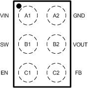
GUID-58179401-4AED-4F66-83A7-44017CDB2637-low.gifFigure 6-1 YFF Package6-Pin YFFTop View
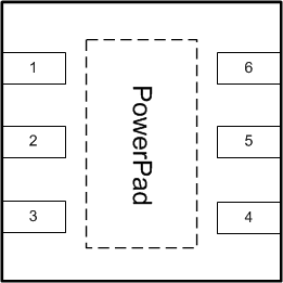
GUID-A4834AC1-87F0-4AE3-9053-335C2EAB2A51-low.gifFigure 6-2 DRV Package6-Pin DRVTop View
Table 6-1 Pin Functions
PIN TYPE DESCRIPTION
NAME YFF DRV
VIN A1 6 I IC power supply input
SW B1 5 PWR Switch pin of the converter. It is connected to the inductor
EN C1 4 I Enable logic input. Logic high voltage enables the device; logic low voltage disables the device. Do not leave it floating.
GND A2 1 PWR Ground
VOUT B2 2 PWR Boost converter output
FB C2 3 I Voltage feedback of adjustable output voltage. Connect to the center tap of a resistor divider to program the output voltage. Connect to GND pin for fixed output voltage versions.
PowerPad 7 Connect to GND