SLVSD88L July 2016 – August 2021 TPS61099
PRODUCTION DATA
- 1 Features
- 2 Applications
- 3 Description
- 4 Revision History
- 5 Device Comparison Table
- 6 Pin Configuration and Functions
- 7 Specifications
- 8 Detailed Description
- 9 Application and Implementation
- 10Power Supply Recommendations
- 11Layout
- 12Device and Documentation Support
- 13Mechanical, Packaging, and Orderable Information
Package Options
Mechanical Data (Package|Pins)
Thermal pad, mechanical data (Package|Pins)
- DRV|6
Orderable Information
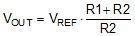
9.2.1.1.2 Programming the Output Voltage
There are two ways to set the output voltage of the TPS61099x. For adjustable output voltage version, select the external resistor divider R1 and R2, as shown in Equation 1, the output voltage is programmed to the desired value. When the output voltage is regulated, the typical voltage at the FB pin is VREF of 1.0 V.
For fixed output voltage versions, the FB pin should be connected to the GND. The TPS61099x offers diverse fixed voltage versions, refer to Device Comparison Table for version details.
In this example, 5-V output is required to bias the memory LCD. For the best accuracy, the current following through R2 should be 100 times larger than FB pin leakage current. Changing R2 towards a lower value increases the robustness against noise injection. Changing R2 towards higher values reduces the FB divider current for achieving the highest efficiency at low load currents. 1-MΩ and 249-kΩ resistors are selected for R1 and R2 in this example. High accuracy resistors are recommended for better output voltage accuracy.