SNVSA40A October 2014 – March 2016 TPS61169
PRODUCTION DATA.
- 1 Features
- 2 Applications
- 3 Description
- 4 Simplified Schematic
- 5 Revision History
- 6 Pin Configuration and Functions
- 7 Specifications
- 8 Detailed Description
- 9 Application and Implementation
- 10Power Supply Recommendations
- 11Layout
- 12Device and Documentation Support
- 13Mechanical, Packaging, and Orderable Information
Package Options
Mechanical Data (Package|Pins)
- DCK|5
Thermal pad, mechanical data (Package|Pins)
Orderable Information
9 Application and Implementation
NOTE
Information in the following applications sections is not part of the TI component specification, and TI does not warrant its accuracy or completeness. TI’s customers are responsible for determining suitability of components for their purposes. Customers should validate and test their design implementation to confirm system functionality.
9.1 Application Information
The TPS61169 device is a step-up DC-DC converter which can drive single or parallel LED strings for small- to large-size panel backlighting. This section includes a design procedure (Detailed Design Procedure) to select component values for the TPS61169 typical application (Figure 4).
9.2 Typical Application
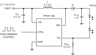 Figure 4. TPS61169 2.7-V to 5.5-V Input, 10 LEDs in Series Output Converter
9.2.1 Design Requirements
For this design example, use the parameters listed in Table 1 as the input parameters.
Table 1. Design Parameters
| DESIGN PARAMETER | EXAMPLE VALUE |
|---|---|
| Input voltage range | 2.7 V to 5.5 V |
| Output, LED number in a string | 10 |
| Output, LED string number | 1 |
| Output, LED current per string | 20 mA |
9.2.2 Detailed Design Procedure
9.2.2.1 Inductor Selection
The selection of the inductor affects power efficiency, steady state operation as well as transient behavior and loop stability. These factors make it the most important component in power regulator design. There are three important inductor specifications, inductor value, DC resistance and saturation current. Considering inductor value alone is not enough. The inductor value determines the inductor ripple current. Choose an inductor that can handle the necessary peak current without saturating. Follow Equation 3 to Equation 4 to calculate the peak current of the inductor. To calculate the current in the worst case, use the minimum input voltage, maximum output voltage and maximum load current of application. In a boost regulator, the input DC current can be calculated as Equation 3.

where
- VOUT = boost output voltage
- IOUT = boost output current
- VIN = boost input voltage
- η = power conversion efficiency
The inductor current peak to peak ripple can be calculated as Equation 4.

where
- ΔIL(PP) = inductor peak-to-peak ripple
- L = inductor value
- FS = boost switching frequency
- VOUT = boost output voltage
- VIN = boost input voltage
Therefore, the peak current IL(P) seen by the inductor is calculated with Equation 5.

Inductor values can have ±20% tolerance with no current bias. When the inductor current approaches saturation level, its inductance can decrease 20% to 35% from the 0-A value depending on how the inductor vendor defines saturation current. Using an inductor with a smaller inductance value forces discontinuous PWM when the inductor current ramps down to zero before the end of each switching cycle. This reduces the boost converter’s maximum output current, causes large input voltage ripple and reduces efficiency. Large inductance value provides much more output current and higher conversion efficiency. For these reasons, a 4.7-μH to 10-μH inductor value range is recommended, and 4.7-μH inductor is recommended for higher than 5-V input voltage by considering inductor peak current and loop stability. Table 2 lists the recommended inductor for the TPS61169.
Table 2. Recommended Inductors for TPS61169
| PART NUMBER | L (µH) | DCR MAX (mΩ) | SATURATION CURRENT (A) | SIZE (L x W x H mm) | VENDOR |
|---|---|---|---|---|---|
| LPS4018-472ML | 4.7 | 125 | 1.9 | 4 × 4 × 1.8 | Coilcraft |
| LPS4018-103ML | 10 | 200 | 1.3 | 4 × 4 × 1.8 | Coilcraft |
| PCMB051H-4R7M | 4.7 | 85 | 4 | 5.4 × 5.2 × 1.8 | Cyntec |
| PCMB051H-100M | 10 | 155 | 3 | 5.4 × 5.2 × 1.8 | Cyntec |
9.2.2.2 Schottky Diode Selection
The TPS61169 demands a low forward voltage, high-speed and low capacitance Schottky diode for optimum efficiency. Ensure that the diode average and peak current rating exceeds the average output current and peak inductor current. In addition, the diode reverse breakdown voltage must exceed the open LED protection voltage. ONSemi NSR0240 is recommended for the TPS61169.
9.2.2.3 Output Capacitor Selection
The output capacitor is mainly selected to meet the requirement for the output ripple and loop stability. This ripple voltage is related to capacitor capacitance and its equivalent series resistance (ESR). Assuming a capacitor with zero ESR, the minimum capacitance needed for a given ripple can be calculated with Equation 6:

where
- Vripple = peak-to-peak output ripple
The additional part of the ripple caused by ESR is calculated using: Vripple_ESR = IOUT × RESR
Due to its low ESR, Vripple_ESR could be neglected for ceramic capacitors, a 1-µF to 4.7-µF capacitor is recommended for typical application.
9.2.2.4 LED Current Set Resistor
The LED current set resistor can be calculated by Equation 1.
9.2.2.5 Thermal Considerations
The allowable IC junction temperature must be considered under normal operating conditions. This restriction limits the power dissipation of the TPS61169. The allowable power dissipation for the device can be determined by Equation 7:

where
- TJ is allowable junction temperature given in recommended operating conditions
- TA is the ambient temperature for the application
- RθJA is the thermal resistance junction-to-ambient given in Power Dissipation Table
The TPS61169 device also features a thermal foldback function to reduce the thermal stress automatically.
9.3 Application Curves
Typical application condition is as in Figure 4, VIN = 3.6 V, RSET = 10.2 Ω, L = 4.7 µH, COUT = 1 µF, 10 LEDs in series (unless otherwise specified).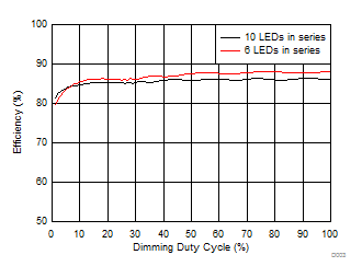

| 8 LEDs in series | ||
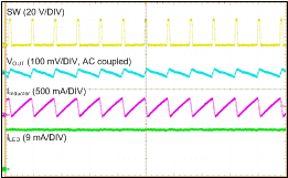
| Time = 1 µs/DIV | ||
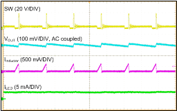
| Time = 2 µs/DIV | ||
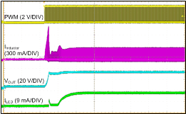
| Time = 2 ms/DIV | ||
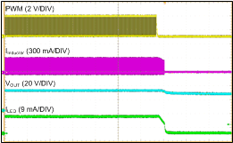
| Time = 2 ms/DIV | ||
| Duty = 50% | ||

| Time = 50 µs/DIV | ||||
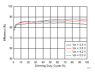
| 10 LEDs in series | ||
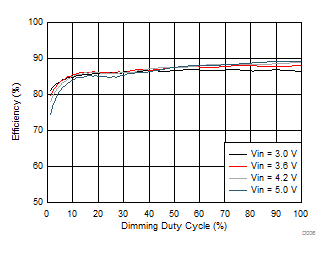
| 6 LEDs in series | ||
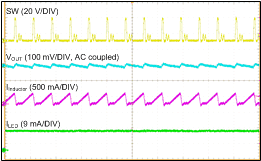
| Time = 1 µs/DIV | ||

| Time = 2 ms/DIV | ||
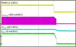
| Time = 2 ms/DIV | ||

| Time = 5 ms/DIV | ||
| Duty = 1%-100%-1% | ||