SLVSAX2B September   2011  – June 2020 TPS61170-Q1

PRODUCTION DATA.  

  1. Features
  2. Applications
  3. Description
    1.     Device Images
      1.      Typical Application
  4. Revision History
  5. Pin Configuration and Functions
    1.     Pin Functions
  6. Specifications
    1. 6.1 Absolute Maximum Ratings
    2. 6.2 ESD Ratings
    3. 6.3 Recommended Operating Conditions
    4. 6.4 Thermal Information
    5. 6.5 Electrical Characteristics
    6. 6.6 Switching Characteristics
    7. 6.7 Typical Characteristics
  7. Detailed Description
    1. 7.1 Overview
    2. 7.2 Functional Block Diagram
    3. 7.3 Feature Description
      1. 7.3.1 Soft Start-up
      2. 7.3.2 Overcurrent Protection
      3. 7.3.3 Undervoltage Lockout
      4. 7.3.4 Thermal Shutdown
      5. 7.3.5 Enable and Shutdown
    4. 7.4 Device Functional Modes
      1. 7.4.1 PWM Program Mode
      2. 7.4.2 1-Wire Program Mode
      3. 7.4.3 EasyScale
    5. 7.5 Programming
      1. 7.5.1 Feedback Reference Program Mode Selection
  8. Application and Implementation
    1. 8.1 Application Information
    2. 8.2 Typical Applications
      1. 8.2.1 12-V to 24-V DC-DC Power Conversion
        1. 8.2.1.1 Design Requirements
        2. 8.2.1.2 Detailed Design Procedure
          1. 8.2.1.2.1 Program Output Voltage
          2. 8.2.1.2.2 Maximum Output Current
          3. 8.2.1.2.3 Switch Duty Cycle
          4. 8.2.1.2.4 Inductor Selection
          5. 8.2.1.2.5 Schottky Diode Selection
          6. 8.2.1.2.6 Compensation Capacitor Selection
          7. 8.2.1.2.7 Input and Output Capacitor Selection
        3. 8.2.1.3 Application Curve
      2. 8.2.2 5-V to 12-V DC-DC Power Conversion With Programmable Feedback Reference Voltage
      3. 8.2.3 12-V SEPIC (Buck-Boost) Converter
  9. Power Supply Recommendations
  10. 10Layout
    1. 10.1 Layout Guidelines
    2. 10.2 Layout Example
    3. 10.3 Thermal Considerations
  11. 11Device and Documentation Support
    1. 11.1 Device Support
      1. 11.1.1 Third-Party Products Disclaimer
    2. 11.2 Documentation Support
      1. 11.2.1 Related Documentation
    3. 11.3 Support Resources
    4. 11.4 Trademarks
    5. 11.5 Electrostatic Discharge Caution
    6. 11.6 Glossary
  12. 12Mechanical, Packaging, and Orderable Information

Package Options

Mechanical Data (Package|Pins)
Thermal pad, mechanical data (Package|Pins)
Orderable Information

12-V SEPIC (Buck-Boost) Converter

The single-ended primary-inductance converter (SEPIC) is a DC-DC converter topology that provides a positive regulated output voltage from an input voltage that varies from above to below the output voltage. In this example, we demonstrate a DC-DC converter that can provide 12 V at 300 mA with 90% efficiency from an input voltage from 9 to 15 V. This converter can be implemented using the TPS61170-Q1 device. See Designing DC/DC converters based on SEPIC topology, SLYT309 for detailed description and application curves.
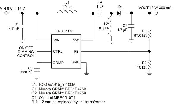
TPS61170-Q1 buck_bst_lvs789.gifFigure 19. 12-V SEPIC (Buck-Boost) Converter