SLVSAX2B September   2011  – June 2020 TPS61170-Q1

PRODUCTION DATA.  

  1. Features
  2. Applications
  3. Description
    1.     Device Images
      1.      Typical Application
  4. Revision History
  5. Pin Configuration and Functions
    1.     Pin Functions
  6. Specifications
    1. 6.1 Absolute Maximum Ratings
    2. 6.2 ESD Ratings
    3. 6.3 Recommended Operating Conditions
    4. 6.4 Thermal Information
    5. 6.5 Electrical Characteristics
    6. 6.6 Switching Characteristics
    7. 6.7 Typical Characteristics
  7. Detailed Description
    1. 7.1 Overview
    2. 7.2 Functional Block Diagram
    3. 7.3 Feature Description
      1. 7.3.1 Soft Start-up
      2. 7.3.2 Overcurrent Protection
      3. 7.3.3 Undervoltage Lockout
      4. 7.3.4 Thermal Shutdown
      5. 7.3.5 Enable and Shutdown
    4. 7.4 Device Functional Modes
      1. 7.4.1 PWM Program Mode
      2. 7.4.2 1-Wire Program Mode
      3. 7.4.3 EasyScale
    5. 7.5 Programming
      1. 7.5.1 Feedback Reference Program Mode Selection
  8. Application and Implementation
    1. 8.1 Application Information
    2. 8.2 Typical Applications
      1. 8.2.1 12-V to 24-V DC-DC Power Conversion
        1. 8.2.1.1 Design Requirements
        2. 8.2.1.2 Detailed Design Procedure
          1. 8.2.1.2.1 Program Output Voltage
          2. 8.2.1.2.2 Maximum Output Current
          3. 8.2.1.2.3 Switch Duty Cycle
          4. 8.2.1.2.4 Inductor Selection
          5. 8.2.1.2.5 Schottky Diode Selection
          6. 8.2.1.2.6 Compensation Capacitor Selection
          7. 8.2.1.2.7 Input and Output Capacitor Selection
        3. 8.2.1.3 Application Curve
      2. 8.2.2 5-V to 12-V DC-DC Power Conversion With Programmable Feedback Reference Voltage
      3. 8.2.3 12-V SEPIC (Buck-Boost) Converter
  9. Power Supply Recommendations
  10. 10Layout
    1. 10.1 Layout Guidelines
    2. 10.2 Layout Example
    3. 10.3 Thermal Considerations
  11. 11Device and Documentation Support
    1. 11.1 Device Support
      1. 11.1.1 Third-Party Products Disclaimer
    2. 11.2 Documentation Support
      1. 11.2.1 Related Documentation
    3. 11.3 Support Resources
    4. 11.4 Trademarks
    5. 11.5 Electrostatic Discharge Caution
    6. 11.6 Glossary
  12. 12Mechanical, Packaging, and Orderable Information

Package Options

Mechanical Data (Package|Pins)
Thermal pad, mechanical data (Package|Pins)
Orderable Information

Pin Configuration and Functions

DRV Package
6-Pin SON With Exposed Thermal Pad
Top View
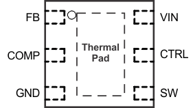
TPS61170-Q1 po_lvs789.gif

Pin Functions

PIN I/O DESCRIPTION
NAME NO.
COMP 2 O Output of the transconductance error amplifier. Connect an external RC network to this pin to compensate the regulator.
CTRL 5 I Control pin of the boost regulator. CTRL is a multi-functional pin which can be used to enable the device and control the feedback voltage with a PWM signal or for digital communications.
FB 1 I Feedback pin for current. Connect to the center tap of a resistor divider to program the output voltage.
GND 3 O Ground
SW 4 I This is the switching node of the IC. Connect SW to the switched side of the inductor.
VIN 6 I The input supply pin for the IC. Connect VIN to a supply voltage between 3 V and 18 V.
Thermal Pad The thermal pad should be soldered to the analog ground plane to avoid thermal issue. If possible, use thermal vias to connect to ground plane for ideal power dissipation.