SLVSCN9B December 2014 – June 2020 TPS61175-Q1
PRODUCTION DATA.
- 1 Features
- 2 Applications
- 3 Description
- 4 Revision History
- 5 Pin Configuration and Functions
- 6 Specifications
- 7 Detailed Description
-
8 Application and Implementation
- 8.1 Application Information
- 8.2
Typical Application
- 8.2.1 Design Requirements
- 8.2.2
Detailed Design Procedure
- 8.2.2.1 Determining the Duty Cycle
- 8.2.2.2 Selecting the Inductor
- 8.2.2.3 Computing the Maximum Output Current
- 8.2.2.4 Setting Output Voltage
- 8.2.2.5 Setting the Switching Frequency
- 8.2.2.6 Setting the Soft Start Time
- 8.2.2.7 Selecting the Schottky Diode
- 8.2.2.8 Selecting the Input and Output Capacitors
- 8.2.2.9 Compensating the Small Signal Control Loop
- 8.2.3 Application Curves
- 9 Power Supply Recommendations
- 10Layout
- 11Device and Documentation Support
- 12Mechanical, Packaging, and Orderable Information
Package Options
Mechanical Data (Package|Pins)
- PWP|14
Thermal pad, mechanical data (Package|Pins)
- PWP|14
Orderable Information
8.2.2.9 Compensating the Small Signal Control Loop
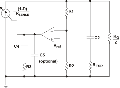
All continuous mode boost converters have a right half plane zero (ƒRHPZ) due to the inductor being removed from the output during charging. In a traditional voltage mode controlled boost converter, the inductor and output capacitor form a small signal double pole. For a negative feedback system to be stable, the fed back signal must have a gain less than 1 before having 180 degrees of phase shift. With its double pole and RHPZ all providing phase shift, voltage mode boost converters are a challenge to compensate. In a converter with current mode control, there are essentially two loops, an inner current feedback loop created by the inductor current information sensed across RSENSE (40 mΩ) and the output voltage feedback loop. The inner current loop allows the switch, inductor and modulator to be lumped together into a small signal variable current source controlled by the error amplifier, as shown in Figure 9.
 Figure 9. Small Signal Model of a Current Mode Boost in CCM
 The new power stage, including the slope compensation, small signal model becomes:

Where


And

He(s) models the inductor current sampling effect as well as the slope compensation effect on the small signal response.
NOTE
If Se slope dominates Sn, that is, when the inductance is oversized in order to give ripple current much smaller than the recommended 0.2 – 0.4 times the average input current, then the converter behaves more like a voltage mode converter, and the above model no longer holds.
The slope compensation in TPS61175-Q1 is shown as follow


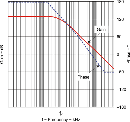
Figure 10 shows a bode plot of a typical CCM boost converter power stage
 Figure 10. Bode Plot of Power Stage Gain and Phase
 The TPS61175-Q1 COMP pin is the output of the internal trans-conductance amplifier. Equation 19 shows the equation for feedback resistor network and the error amplifier.

where GEA and REA are the amplifier’s trans-conductance and output resistance located in the Electrical Characteristics table.


and

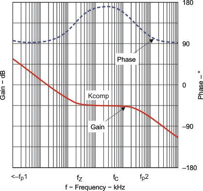
Figure 11 shows a typical bode plot for transfer function H(s).
 Figure 11. Bode Plot of Feedback Resistors and Compensated Amplifier Gain and Phase
 The next step is to choose the loop crossover frequency, fC. The higher in frequency that the loop gain stays above zero before crossing over, the faster the loop response will be and therefore the lower the output voltage will droop during a step load. It is generally accepted that the loop gain cross over no higher than the lower of either 1/5 of the switching frequency, fSW, or 1/3 of the RHPZ frequency, fRHPZ. To approximate a single pole roll-off up to fP2, select R3 so that the compensation gain, KCOMP, at fC on Figure 11 is the reciprocal of the gain, KPW, read at frequency fC from the Figure 10 bode plot or more simply
KCOMP(fC) = 20 × log(GEA × R3 × R2/(R2+R1)) = 1/KPW(fC)
This makes the total loop gain, T(s) = GPS(s) × HEA(s), zero at the fC. Then, select C4 so that fZ ≅ fC/10 and optional fP2> fC *10. Following this method should lead to a loop with a phase margin near 45 degrees. Lowering R3 while keeping fZ ≅ fC/10 increases the phase margin and therefore increases the time it takes for the output voltage to settle following a step load.
In the TPS61175-Q1, if the FB pin voltage changes suddenly due to a load step on the output voltage, the error amplifier increases its transconductance for 8-ms in an effort to speed up the IC’s transient response and reduce output voltage droop due to the load step. For example, if the FB voltage decreases 10-mV due to load change, the error amplifier increases its source current through COMP by 5 times; if FB voltage increases 11-mV, the sink current through COMP is increased to 3.5 times normal value. This feature often results in saw tooth ringing on the output voltage, shown as Figure 13. Designing the loop for greater than 45 degrees of phase margin and greater than 10db gain margin minimizes the amplitude of this ringing. This feature is disabled during soft start.