SLVSDA7E February   2017  – August 2019 TPS61178

PRODUCTION DATA.  

  1. Features
  2. Applications
  3. Description
    1.     Device Images
      1.      Typical Application
  4. Revision History
  5. Device Comparison Table
  6. Pin Configuration and Functions
    1.     Pin Functions
  7. Specifications
    1. 7.1 Absolute Maximum Ratings
    2. 7.2 ESD Ratings
    3. 7.3 Recommended Operating Conditions
    4. 7.4 Thermal Information
    5. 7.5 Electrical Characteristics
    6. 7.6 Timing Requirements
    7. 7.7 Switching Characteristics
    8. 7.8 Typical Characteristics
  8. Detailed Description
    1. 8.1 Overview
    2. 8.2 Functional Block Diagram
    3. 8.3 Feature Description
      1. 8.3.1  Under-voltage Lockout
      2. 8.3.2  Enable and Disable
      3. 8.3.3  Startup
      4. 8.3.4  Load Disconnect Gate Driver
      5. 8.3.5  Adjustable Peak Current Limit
      6. 8.3.6  Output Short Protection (with load disconnected FET)
      7. 8.3.7  Adjustable Switching Frequency
      8. 8.3.8  External Clock Synchronization (TPS611781)
      9. 8.3.9  Error Amplifier
      10. 8.3.10 Slope Compensation
      11. 8.3.11 Start-up with the Output Pre-Biased
      12. 8.3.12 Bootstrap Voltage (BST)
      13. 8.3.13 Over-voltage Protection
      14. 8.3.14 Thermal Shutdown
    4. 8.4 Device Functional Modes
      1. 8.4.1 Operation
      2. 8.4.2 Auto PFM Mode (TPS61178)
      3. 8.4.3 Forced PWM Mode (TPS611781)
  9. Application and Implementation
    1. 9.1 Application Information
    2. 9.2 Typical Application
      1. 9.2.1 Design Requirements
      2. 9.2.2 Detailed Design Procedure
        1. 9.2.2.1 Custom Design With WEBENCH® Tools
        2. 9.2.2.2 Setting the Switching Frequency
      3. 9.2.3 Setting the Current Limit
      4. 9.2.4 Setting the Output Voltage
        1. 9.2.4.1 Selecting the Inductor
        2. 9.2.4.2 Selecting the Output Capacitors
        3. 9.2.4.3 Selecting the Input Capacitors
        4. 9.2.4.4 Loop Stability and Compensation
          1. 9.2.4.4.1 Small Signal Model
          2. 9.2.4.4.2 Loop Compensation Design Steps
          3. 9.2.4.4.3 Selecting the Disconnect FET
          4. 9.2.4.4.4 Selecting the Bootstrap Capacitor
          5. 9.2.4.4.5 VCC Capacitor
      5. 9.2.5 TPS61178 Application Waveform
    3. 9.3 System Examples
      1. 9.3.1 TPS61178 with 14-V Output from 2.7-V to 4.4-V Input Voltage
      2. 9.3.2 TPS61178 Without Load Disconnect Function
      3. 9.3.3 TPS611781 External Clock Synchronization
  10. 10Power Supply Recommendations
  11. 11Layout
    1. 11.1 Layout Guidelines
    2. 11.2 Layout Example
  12. 12Device and Documentation Support
    1. 12.1 Device Support
      1. 12.1.1 Third-Party Products Disclaimer
      2. 12.1.2 Development Support
        1. 12.1.2.1 Custom Design With WEBENCH® Tools
    2. 12.2 Documentation Support
      1. 12.2.1 Related Documentation
    3. 12.3 Related Links
    4. 12.4 Receiving Notification of Documentation Updates
    5. 12.5 Community Resources
    6. 12.6 Trademarks
    7. 12.7 Electrostatic Discharge Caution
    8. 12.8 Glossary
  13. 13Mechanical, Packaging, and Orderable Information

Package Options

Mechanical Data (Package|Pins)
Thermal pad, mechanical data (Package|Pins)
Orderable Information

Typical Characteristics

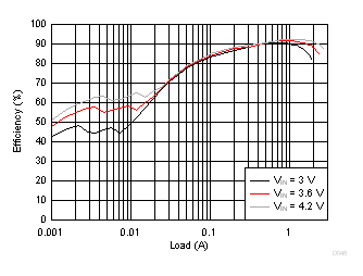
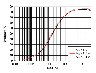
TPS61178 D042_SLVSDA7.gif
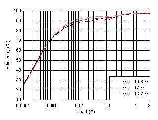
VOUT = 16 V L = 3.3 µH Auto PFM
Figure 1. Efficiency vs. Output Current
TPS61178 D046_SLVSDA7.gif
VOUT = 14 V L = 1.8 µH Auto PFM
Figure 3. Efficiency vs. Output Current
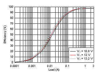
TPS61178 D045_SLVSDA7.gif
VOUT = 16 V L = 3.3 µH Forced PWM
Figure 5. Efficiency vs. Output Current
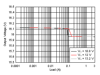
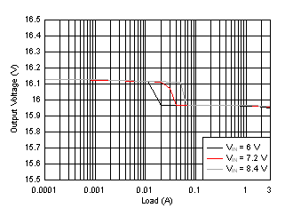
TPS61178 D048_SLVSDA7.gif
VOUT = 16 V L = 3.3 µH Auto PFM
Figure 7. Output Voltage vs. Load
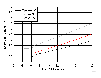
TPS61178 D018_SLVSDA7.gif
Figure 9. Shutdown Current vs VIN
TPS61178 D014_SLVSDA7.gif
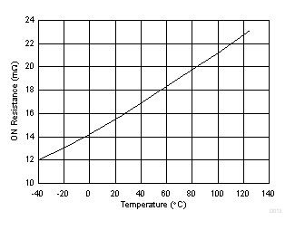
VCC = 6 V
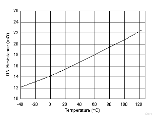
Figure 11. LS Rdson vs Temperature
TPS61178 D032_SLVSDA7.gif
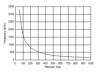
VIN = 7.2 V VOUT = 16 V
Figure 13. Frequency vs Setting Resistor
TPS61178 D023_SLVSDA7.gif
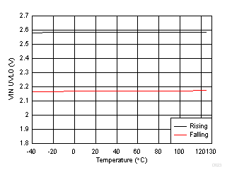
Figure 15. VIN UVLO Rising / Falling vs Temperature
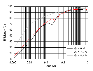
TPS61178 D043_SLVSDA7.gif
VOUT = 16 V L = 3.3 µH Auto PFM
Figure 2. Efficiency vs. Output Current
TPS61178 D044_SLVSDA7.gif
VOUT = 16 V L = 3.3 µH Forced PWM
Figure 4. Efficiency vs. Output Current
TPS61178 D047_SLVSDA7.gif
VOUT = 16 V L = 3.3 µH Auto PFM
Figure 6. Output Voltage vs. Load
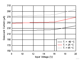
TPS61178 D034_SLVSDA7.gif
Figure 8. Quiescent Current vs VIN
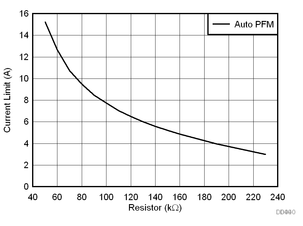
TPS61178 D040_SLVSDA7.gif
VOUT = 16 V VIN = 7.2 V Auto PFM
Figure 10. Switch Current Limit vs Setting Resistor
TPS61178 D013_SLVSDA7.gif
VCC = 6 V
Figure 12. HS Rdson vs Temperature
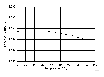
TPS61178 D015_SLVSDA7.gif
Figure 14. Reference Voltage vs Temperature
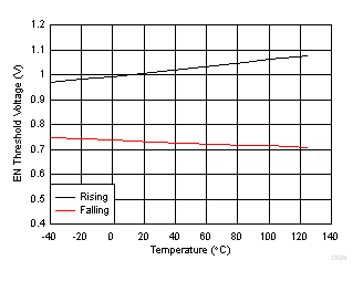
TPS61178 D024_SLVSDA7.gif
Figure 16. EN Threshold Rising / Falling vs Temperature