SLVSAO4C December   2010  – June 2020 TPS61240-Q1

PRODUCTION DATA.  

  1. Features
  2. Applications
  3. Description
    1.     Simplified Schematic
  4. Revision History
  5. Pin Configuration and Functions
    1.     Pin Functions
  6. Specifications
    1. 6.1 Absolute Maximum Ratings
    2. 6.2 ESD Ratings
    3. 6.3 Recommended Operating Conditions
    4. 6.4 Thermal Information
    5. 6.5 Electrical Characteristics
    6. 6.6 Typical Characteristics
  7. Detailed Description
    1. 7.1 Overview
    2. 7.2 Functional Block Diagram
    3. 7.3 Feature Description
      1. 7.3.1 Current Limit Operation
      2. 7.3.2 Undervoltage Lockout
      3. 7.3.3 Input Overvoltage Protection
      4. 7.3.4 Enable
      5. 7.3.5 Soft Start
      6. 7.3.6 Load Disconnect
      7. 7.3.7 Thermal Shutdown
    4. 7.4 Device Functional Modes
      1. 7.4.1 Power-Save Mode
  8. Application and Implementation
    1. 8.1 Application Information
    2. 8.2 Typical Applications
      1. 8.2.1 Design Requirements
      2. 8.2.2 Detailed Design Procedure
        1. 8.2.2.1 Programming the Output Voltage
        2. 8.2.2.2 Inductor Selection
        3. 8.2.2.3 Input Capacitor
        4. 8.2.2.4 Output Capacitor
        5. 8.2.2.5 Checking Loop Stability
      3. 8.2.3 Application Curves
    3. 8.3 System Example
  9. Power Supply Recommendations
  10. 10Layout
    1. 10.1 Layout Guidelines
    2. 10.2 Layout Example
  11. 11Device and Documentation Support
    1. 11.1 Documentation Support
      1. 11.1.1 Related Documentation
    2. 11.2 Receiving Notification of Documentation Updates
    3. 11.3 Community Resources
    4. 11.4 Trademarks
    5. 11.5 Electrostatic Discharge Caution
    6. 11.6 Glossary
  12. 12Mechanical, Packaging, and Orderable Information

Package Options

Mechanical Data (Package|Pins)
Thermal pad, mechanical data (Package|Pins)
Orderable Information

Application Curves

Table 3. Table of Application Curves

Figure
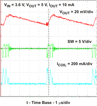
Waveforms Output voltage ripple, PFM mode, IOUT = 10 mA Figure 10
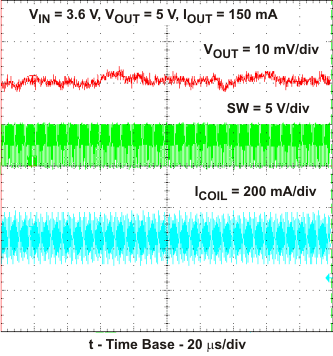
Output voltage ripple, PWM mode, IOUT = 150 mA Figure 11
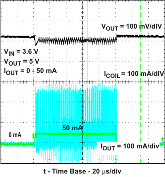
Load transient response, VIN, 3.6 V, 0 mA to 50 mA Figure 12
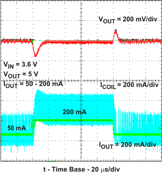
Load transient response, VIN, 3.6 V, 50 mA to 200 mA Figure 13
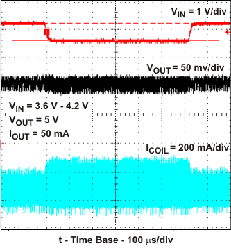
Line transient response, VIN, 3.6 V to 4.2 V, IOUT = 50 mA Figure 14
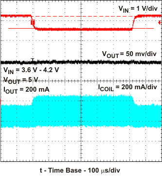
Line transient response, VIN, 3.6 V to 4.2 V, IOUT = 200 mA Figure 15
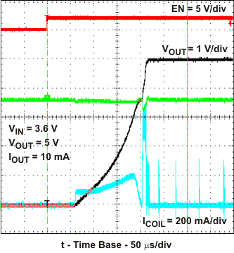
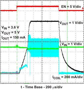
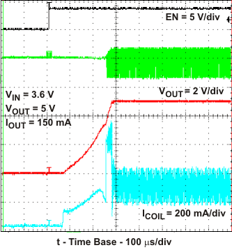
Startup after enable, VIN, 3.6 V, VOUT = 5 V, Load = 5 kΩ Figure 16
Startup after enable, VIN, 3.6 V, VOUT = 5 V, Load = 16.5 kΩ Figure 17
Startup and shutdown, VIN, 3.6 V, VOUT = 5 V, Load = 16.5 kΩ Figure 18
TPS61240-Q1 pfm_ripple_lvs806.gif
Figure 10. Output Voltage Ripple – PFM Mode
TPS61240-Q1 load_trns_lvs806.gif
Figure 12. Load Transient Response
0 mA to 50 mA and 50 mA to 0 mA
TPS61240-Q1 line_trns_lvs806.gif
Figure 14. Line Transient Response
3.6 V to 4.2 V at 50 mA Load
TPS61240-Q1 start_no_load_lvs806.gif
Figure 16. Startup After Enable – No Load
TPS61240-Q1 stsh_w_load_lvs806.gif
Figure 18. Startup and Shutdown
TPS61240-Q1 pwm_ripple_lvs806.gif
Figure 11. Output Voltage Ripple – PWM Mode
TPS61240-Q1 load_trns3_lvs806.gif
Figure 13. Load Transient Response
0 mA to 200 mA and 200 mA to 0 mA
TPS61240-Q1 line_trns3_lvs806.gif
Figure 15. Line Transient Response
3.6 V to 4.2 V at 200 mA Load
TPS61240-Q1 start_w_load_lvs806.gif
Figure 17. Startup After Enable – With Load