SLVSAO4C December   2010  – June 2020 TPS61240-Q1

PRODUCTION DATA.  

  1. Features
  2. Applications
  3. Description
    1.     Simplified Schematic
  4. Revision History
  5. Pin Configuration and Functions
    1.     Pin Functions
  6. Specifications
    1. 6.1 Absolute Maximum Ratings
    2. 6.2 ESD Ratings
    3. 6.3 Recommended Operating Conditions
    4. 6.4 Thermal Information
    5. 6.5 Electrical Characteristics
    6. 6.6 Typical Characteristics
  7. Detailed Description
    1. 7.1 Overview
    2. 7.2 Functional Block Diagram
    3. 7.3 Feature Description
      1. 7.3.1 Current Limit Operation
      2. 7.3.2 Undervoltage Lockout
      3. 7.3.3 Input Overvoltage Protection
      4. 7.3.4 Enable
      5. 7.3.5 Soft Start
      6. 7.3.6 Load Disconnect
      7. 7.3.7 Thermal Shutdown
    4. 7.4 Device Functional Modes
      1. 7.4.1 Power-Save Mode
  8. Application and Implementation
    1. 8.1 Application Information
    2. 8.2 Typical Applications
      1. 8.2.1 Design Requirements
      2. 8.2.2 Detailed Design Procedure
        1. 8.2.2.1 Programming the Output Voltage
        2. 8.2.2.2 Inductor Selection
        3. 8.2.2.3 Input Capacitor
        4. 8.2.2.4 Output Capacitor
        5. 8.2.2.5 Checking Loop Stability
      3. 8.2.3 Application Curves
    3. 8.3 System Example
  9. Power Supply Recommendations
  10. 10Layout
    1. 10.1 Layout Guidelines
    2. 10.2 Layout Example
  11. 11Device and Documentation Support
    1. 11.1 Documentation Support
      1. 11.1.1 Related Documentation
    2. 11.2 Receiving Notification of Documentation Updates
    3. 11.3 Community Resources
    4. 11.4 Trademarks
    5. 11.5 Electrostatic Discharge Caution
    6. 11.6 Glossary
  12. 12Mechanical, Packaging, and Orderable Information

Package Options

Mechanical Data (Package|Pins)
Thermal pad, mechanical data (Package|Pins)
Orderable Information

Current Limit Operation

The current limit circuit employs a valley current sensing scheme. Current limit detection occurs during the off time through sensing of the voltage drop across the synchronous rectifier.

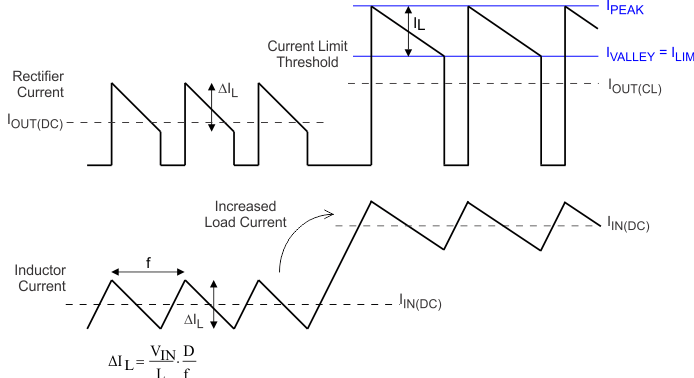
During the current limit operation, the output voltage is reduced as the power stage of the device operates in a constant current mode. The maximum continuous output current (IOUT(CL)), before entering current limit operation, can be defined by Equation 1.

Equation 1. TPS61240-Q1 eq1_iout_lvs806.gif

Figure 8 illustrates the inductor and rectifier current waveforms during current limit operation. The output current, IOUT, is the average of the rectifier ripple current waveform. When the load current is increased such that the lower peak is above the current limit threshold, the off time is lengthened to allow the current to decrease to this threshold before the next on-time begins (so called frequency fold-back mechanism).
TPS61240-Q1 ind_cur_lvsag8.gifFigure 8. Inductor/Rectifier Currents in Current Limit Operation