SLVSFP3C August 2020 – March 2022 TPS61288
PRODUCTION DATA
- 1 Features
- 2 Applications
- 3 Description
- 4 Revision History
- 5 Device Comparison
- 6 Pin Configuration and Functions
- 7 Specifications
- 8 Detailed Description
- 9 Application and Implementation
- 10Power Supply Recommendations
- 11Layout
- 12Device and Documentation Support
- 13Mechanical, Packaging, and Orderable Information
Package Options
Mechanical Data (Package|Pins)
- RQQ|11
Thermal pad, mechanical data (Package|Pins)
Orderable Information
6 Pin Configuration and Functions
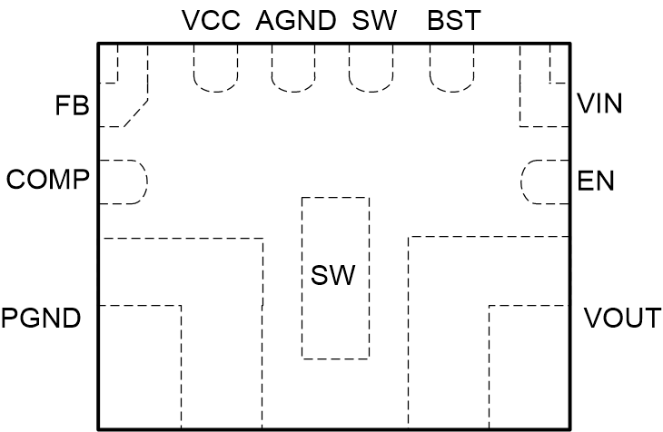
 Figure 6-1 11-Pin RQQ VQFN Package (Top
View)
Figure 6-1 11-Pin RQQ VQFN Package (Top
View)Table 6-1 Pin Functions
| PIN | I/O | DESCRIPTION | |
|---|---|---|---|
| NAME | NUMBER | ||
| FB | 1 | I | Voltage feedback. Connect to the center tape of a resistor divider to program the output voltage. |
| COMP | 2 | O | Output of the internal error amplifier, the loop compensation network should be connected between this pin and the AGND pin. |
| PGND | 3 | PWR | Power ground of the IC. It is connected to the source of the low-side MOSFET. |
| SW | 4,9 | PWR | The switching node pin of the converter. It is connected to the drain of the internal low-side power MOSFET and the source of the internal high-side power MOSFET. |
| VOUT | 5 | PWR | Boost converter output |
| EN | 6 | I | Enable logic input. Logic high level enables the device. Logic low level disables the device and turns it into shutdown mode. |
| VIN | 7 | I | IC power supply input |
| BST | 8 | O | Power supply for high-side MOSFET gate driver. A ceramic capacitor of 0.1 µF must be connected between this pin and the SW pin. |
| AGND | 10 | - | Signal ground of the IC |
| VCC | 11 | O | Output of the internal regulator. A ceramic capacitor of more than 1.0 µF is required between this pin and ground. |